

I’m currently contemplating an unusual annual technical conference. This affair is invitation only. Attendance is limited to 100 people give-or-take. In addition to the leading computer chip architects from companies like Intel and AMD, it’s also common to rub shoulders with pioneers of technology spanning everything from computing to electric vehicles to deep space exploration. This conference, whose name I may not speak, is held at a facility in a location I may not reveal, but I fear I’ve said too much.
I’m sure you’ve heard the old advice for giving presentations: “(1) Tell them what you are going to tell them, (2) Tell them, and (3) Tell them what you just told them.” When I was first invited to speak at this conference, I was told to only cover point (2) and also to cut out anything extraneous because “They will get it!”
I’ve met all sorts of interesting people at this conference. For example, I met one of the guys who designed the first commercial microprocessor in the form of the Intel 4004, one of the guys who created VisiCalc (the first spreadsheet program for personal computers), the guy who invented the Forth programming language, and… the list goes on.
In addition to the technical presentations, there are myriad interesting demos and discussions. One year, for example, one of the guys who invented the Furby attended the conference following this toy’s holiday season launch to talk about how this little beauty came to be, including the way he and his partner had defined and implemented the Furbish language.
I remember one year during a lunch break watching in awe as a young lady fabricated a transistor by hand using a miniature furnace. Once the device had cooled and she’d attached wires, she demonstrated its amplification characteristics using a multimeter. I’m not sure (memories fade over time), but I think the presenter in question may have been Jeri Ellsworth.
The reason I mention Jeri is that I was just re-reading Sam Zeloof’s article about how he created his first homemade integrated circuit (Sam referenced Jeri’s work in his article, thereby triggering my cascade of thoughts above).
Do you recall my recent column Are We Ready for the 2nm Process Node? Well, Sam’s work could be characterized as being at the 175µm technology node, which in no way detracts from his awesome achievement.
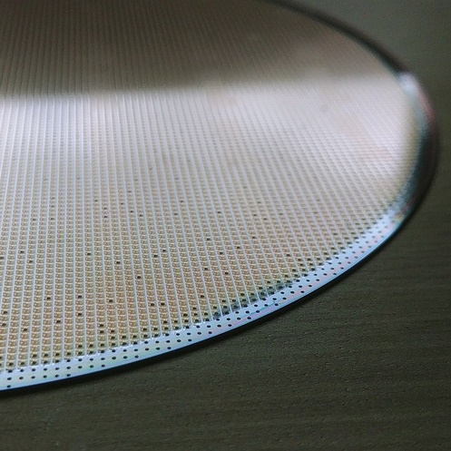
If you are a mega-corporation (well, not you personally, but you know what I mean) like Intel, you may have your own semiconductor fabrication facilities, also known as foundries or fabs. If you are a medium-sized fabless company, you may design your devices and then use one of the big fabs like TSMC to build and package your chips for you. But what do you do if you are a small company, or a university department, and you wish to create a bunch of integrated circuits?
There are Shuttle Programs, also known as Multi-Project Wafer Services, such as the Multi-Project Wafer (MPW) Shuttle Program from Tower Semiconductor or the Silicon Shuttle offering from UMC. The idea here is that instead of the wafer carrying multiple copies of the same design for a single customer, it contains a few copies of multiple designs submitted by multiple customers. In this case, companies share the costs of mask creation and wafer fabrication, with each company receiving only a handful of their chips. This is ideal for educational and prototyping projects, but what do you do if you need more?
I’m glad you asked. I was just chatting with Phil Yoon, who is the Founder and Director of Research and Business Development at a foundry called SynchroLux, which is based in South Korea.
Phil explained how SynchroLux is small, feisty, and ideally suited to fulfilling the early-stage prototyping and low-volume production projects that are the hallmark of small design houses. Furthermore, Phil notes that once a design has matured, the folks at SynchroLux can proceed with time-effective production in high volume.
As an example, Phil noted that if a small company were to approach a behemoth like TSMC, it could be months or years before their project managed to work its weary way into the schedule. By comparison, Phil notes that SynchroLux could be up and running on the project within a week of receiving the purchase order.
Processing services are available on wafers of 4”, 5”, 6”, 8” (200mm) and 12” (300mm) in diameter. In addition to standard CMOS, SynchroLux also offers power semiconductors based on silicon carbide (SiC) and gallium nitride (GaN).
SynchroLux predominantly works at the 180nm process node (they can offer electron-beam lithography down to 15nm for those that need it). Now, the 180nm node may sound “chunky and clunky” if you are used to hearing about the latest and greatest ASIC technologies, but there is a huge market (and associated chip shortages) for devices manufactured using tried-and-tested “mature” processes like the 180nm node.
In addition to semiconductor devices, SynchroLux also has a dedicated MEMS team with deep experience and expertise in the fabrication of MEMS devices like sensors, mirrors, photonics, and microfluidics. As opposed to simply taking your completed designs and implementing them, the guys and gals at SynchroLux are happy to work with you to create custom semiconductors, sensors, and imaging devices.
But wait, there’s more, because the folks at SynchroLux also offer packaging services, making them a true one-stop-shop. You send them your design, and they respond by sending you your packaged devices. As Phil said to me: “We are capable of producing a variety of semiconductor devices using standard IC and CMOS technologies in a fraction of the time and at a fraction of the cost of large foundries, all without any compromises in quality.”
Writing about all of this just triggered another thought in my poor old noggin. Recently, I’ve grown interested in the concept of cheeky little chiplets (see Are You Ready for the Chiplet Age? and Chiplets for the Unwashed Masses and Is This the Ultimate Chiplet Interconnect Technology? and Is This the Future of Chiplet-Based Design? and Infineon and Archetype to Develop AI Sensor Chipsets). So, what I was just thinking was that if someone were interested in creating a library of chiplets that people could start playing with, they could do worse than teaming with a lean, mean, affordable, and fast foundry like SynchroLux.
What say you? Do you have any thoughts you’d care to share on anything you’ve read here? If nothing else, what do you think about Sam Zeloof and his homemade silicon chip?


One thought on “Want to Create Silicon Chips? Want Them Fast? Want them Cheap?”