

Do you ever get the feeling you are sitting on the cusp of a new era, metaphorically speaking? That’s the way I currently feel with respect to chiplets (I only wish I was gowned in garb apposite to the occasion).
The concept of chiplets has been around for some time, and they’ve been in use for the past few years, but only by big players like Intel, for example, who have humongous resources and who can control every aspect of chiplet development and deployment. Now it seems that chiplet technology is poised to be made available to the unwashed masses (e.g., me and my friends).
To be honest, this has been heading our way for some time now. In my recent Are You Ready for the Chiplet Age? column, we noted that the maximum practical size for a silicon die is around 600mm2 (approximately 25mm x 25mm). We can make larger chips—topping out around 850mm2 (approximately 29mm x 29mm)—but the fall in yield will bring tears to your eyes.
The solution is to take multiple dice, mount them on a common substrate, and present everything in a single package, which may be referred to as a “multi-die system.” In this case, the dice are commonly referred to as “chiplets” or “tiles.”
To date, there have been four main use-cases for chiplet technologies as follows:
- You may decide to simply mount a bunch of homogeneous chiplets (think processors like CPUs, GPUs, NPUs, etc.) on the same substrate.
- Suppose you are designing a device that you would ideally like to create as a single ginormous die, but you can’t because it would exceed the 600mm2 limit. In this case, you might split its functionality across several smaller chiplets.
- You may have specific functions, like transceivers, that have been implemented and rigorously tested at an earlier process node and that won’t benefit from being reimplemented at a more advanced node. In this case, you may decide to implement these functions as small chiplets that surround a core die implemented at the latest-and-greatest technology node.
- You may opt to disaggregate everything into heterogeneous dice implemented at the best nodes (in terms of cost, power, etc.) for those functions. For example, an RF die implemented using a 28nm process, analog-to-digital converters (ADCs) implemented in a 16nm process, and digital logic implemented in a 5nm process.
There is also a fifth use case—one that is of particular interest in the context of this column—but we will come to that in a moment. With respect to the four use cases above, as noted earlier, these have traditionally been of interest only to big players who have humongous resources and who can control every aspect of chiplet development and deployment.
One example that springs to mind in the case of scenario 3 is offered by Intel Agilex 7 FPGAs and SoC FPGAs, which contain two to six transceiver (XCVR) chiplets in addition to the main die. Meanwhile, in the case of scenario 4, may I make so bold as to present the Intel Data Center GPU Max Series of devices (these used to be known as Ponte Vecchio GPUs) that flaunt 47 tiles and 100+ billion transistors.
I’ve been seeing a lot of activity on the chiplet front recently. For example, the guys and gals at Ayar Labs are doing some very interesting work with in-package optical interconnect involving chiplets that combine photonic and electronic functionality. The photonic side provides optical interconnect to the outside world, while the electronic side talks to the main die.
Another interesting company is Arteris IP, who provide state-of-the-art network-on-chip (NoC) interconnect IP. As I mentioned in my Cheeky Chiplets Meet Super NoCs column, the chaps and chapesses at Arteris are doing some very interesting work with respect to “Super NoCs” that can be employed in the context of die-to-die (D2D) chiplet interconnect in multi-die systems.
The long-term promise of chiplet technology is for smaller companies to be able purchase chiplet IPs—that is, IP functions like an FPGA, a processor, and a memory—and connect them together like LEGO blocks to (relatively) quickly and easily create their own multi-die systems. This would be a fifth usage model to add to the four we introduced above.
If you’d asked me about this yesterday, I would have hazarded a guess that this capability was more than a few years in our future. If you were to ask me today, however, I would say that it’s going to be available to us sooner than you think. How soon? Read on…
I was just chatting with Kash Johal, who is the CEO at YorChip, and Brian Faith, who is President and CEO at QuickLogic. Now, this is where you really need to sit up and pay attention, because keeping track of who is doing what to who can quickly become confusing (it’s a bit like watching someone doing the shell game involving three shells and a pea).
As you will doubtless recall, QuickLogic is the leading provider of open reconfigurable computing solutions based on 100% open-source software and hardware. In addition to a bunch of other stuff, the folks at QuickLogic sell off-the-shelf FPGAs and embedded FPGA (eFPGA) IP that other developers can include in their own system-on-chip (SoC) designs. Meanwhile, YorChip is a Silicon Valley-based start-up focused on developing chiplets for mass markets. In addition to their chiplet expertise, the folks at YorChip are black belts at chiplet-to-chiplet interconnect using Universal Chiplet Interconnect Express (UCIe).
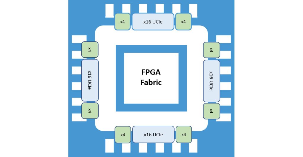
So, the folks at YorChip have taken a 40,000-look-up table (LUT) eFPGA IP from QuickLogic, surrounded it with a terabit of UCIe input/output (I/O) UCIe bandwidth, and augmented this with their own low latency fabric, all resulting in a cheeky little chiplet.
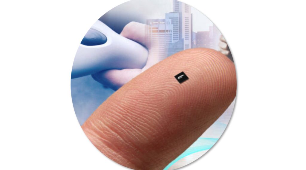
A cheeky little FPGA chiplet (Source: YorChip)
There’s a lot more to things than this, of course. For example, multiple chiplets can be connected, allowing you to build up to a 6 x 6 array (36 FPGA chiplets) to give 1M+ LUT capacity. These cheeky chiplets can be provided as raw (bare) die or in a chip scale package (CSP) form factor. As a first step towards dipping their toes in the chiplet waters, developers will be able to use packaged chiplets on standard printed circuit boards (PCBs), thereby saving years in terms of time to market and millions of dollars in NRE.
A YorChip FPGA chiplet presented is a CSP (Source: YorChip)
This is where the shell game returns to mind, because YorChip isn’t going to sell these chiplets itself. Since YorChip is the expert in UCIe IP and what it takes to design chiplets, it is taking the lead in developing the FPGA chiplet. By comparison, since QuickLogic is the expert in FPGAs, eFPGA IP, and FPGA User Tools, it will be the one selling/supporting the FPGA chiplets (in both raw die and CSP form). This makes sense on multiple levels, not least that QuickLogic already supplies and supports its Aurora Software Tool Suite for eFPGA Design, where these tools are based on 100% open-source components such as Yosys, VPR, and FOEDAG.
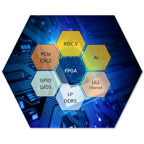
But wait, there’s more, because the folks at YorChip are actively engaging with other companies to create a chiplet ecosystem, starting with a RISC-V chiplet, an artificial intelligence (AI) chiplet, an LP DDR5 chiplet, and so forth.
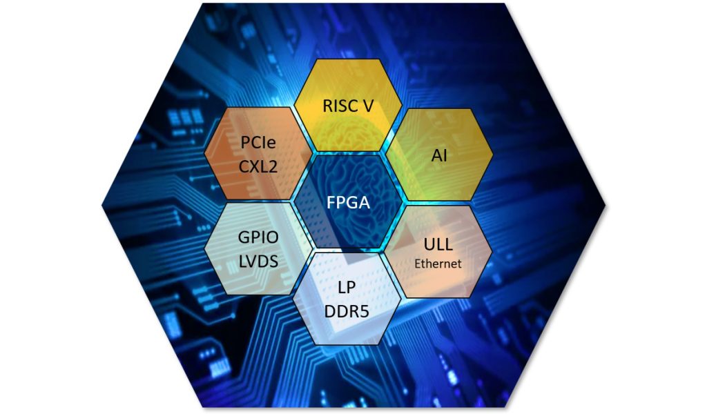
Some of the additional chiplets that are in the works (Source: YorChip)
Once again, YorChip is focused on accelerating the chiplet ecosystem via its UCIe IP and its expertise in chiplet design. The “storefront” responsibility for selling and supporting the various chiplets will primarily fall on the partner companies (e.g., the RISC-V Company for the RISC-V chiplet, the memory company for the memory chiplet, etc.). As Kash told me, “This leverages all the companies’ strengths while building out the ecosystem that the chiplet market so desperately needs to gain scale outside of the few large companies that use chiplet technology today for internal use only.” I couldn’t have said it better myself.
So, how close are we to this chiplet Nirvana and this silicon Shangri-La? Well, we aren’t quite there yet (which is why you won’t currently find these little scamps on the QuickLogic website or in its store). My understanding is that developers will be able to start… well, developing… in early 2024, with silicon (chiplets) coming available in the first half of 2025.
Although this may seem a long time away as you read this, experience has shown me that we’ll be hurtling through 2025 before we know it (which is awkward because I don’t have a speech prepared and I’ve got nothing to wear). What say you? Do you have any thoughts you’d care to share on anything you’ve read here?


