

As is usually the case, I’m astonished and astounded by the leaps in technology that are occurring all around me. Things are now moving so fast that there will probably be yet another mindboggling development before I’ve finished this column (so I’d better write it as quickly as I can).
The generation of electronics engineers that came before your humble narrator (as you know, I pride myself on my humility) were obliged to work their magic with discrete transistors. I was fortunate to come up in the time of “jellybean” digital silicon chips, each of which contained a handful of relatively simple functions ranging from primitive logic gates to things like shift registers and 4-bit arithmetic logic units (ALUs).
The sort of thing we are talking about here are bipolar junction transistor (BJT)-based SN7400-series integrated circuits (ICs), which were presented to the market by Texas Instruments (TI) circa the mid-1960s, and complementary metal-oxide semiconductor (CMOS)-based 4000-series devices, which were introduced by RCA in 1968.
I remember circuit boards circa the 1980s that were around 30” x 24” in size carrying hundreds of these little scamps. The number of logic gates that could be squeezed onto an IC increased over time. This led to smaller circuit boards carrying fewer components. I remember that we used to employ the acronyms SSI, MSI, LSI, VLSI, and ULSI to represent Small-, Medium-, Large-, Very-Large-, and Ultra-Large-Scale Integration, respectively. By one convention, the number of primitive gates represented by these terms were: SSI (1-12), MSI (13-99), LSI (100-999), VLSI (1,000-999,999), and ULSI (1,000,000 or more).
To provide a point of reference, when we talk about primitive gates in this context, it is common to use the term “equivalent gate.” It is also common for a 2-input NAND function to serve as the equivalent gate, where a CMOS implementation of a NAND requires four transistors. Having said this, I also recall a more esoteric convention that defined an emitter-coupled logic (ECL) equivalent gate as being “one-eleventh the minimum logic required to implement a single-bit full-adder” (give me strength).
I designed my first ASIC circa 1980. This was a gate-array (GA) device, which was implemented at the 5-micron (µm) technology node and contained only 300 equivalent gates (i.e., 1,200 transistors). When we say, “technology node,” and qualify it with a number, this value reflects the size of the smallest structures that can be fabricated in the silicon (actually, things are a bit more complex than this, but we don’t want to wander off into the weeds).
I think it was around 1990 when we (the human race, not me and my friends) reached the 1µm technology node, by which time the naysayers were in full cry, saying: “We’ve reached the end of the line. It isn’t possible to go smaller than this!” Of course, hindsight is the only exact science. As we now know, it wasn’t long before we achieved 900 nanometers (nm), which is 0.9µm, then 800nm, then 700nm… Today, companies at the cutting edge are working at 10nm and 7nm; companies at the bleeding edge are working at 5nm; the 3nm technology node is poised to pounce; and the 2nm and 1nm nodes are lurking in the not-so-distant-future-in-the-scheme-of-things, as it were.
As a rule-of-thumb, smaller transistors switch faster and consume less power (again, I’m simplifying things a tad). Also, shrinking the size of the transistors means you can squeeze more of the little scamps into the same area on the silicon.
In the context of ICs, the term “monolithic” refers to a device in which everything is implemented on a single piece of silicon, which is called a die. Thus far, following Moore’s Law, and as a function of the introduction of new technology nodes, the number of transistors that can be created on a die has been doubling approximately every two years. As a result, Apple’s A16 Bionic system-on-chip (SoC) device, which was introduced in 2022, contains a staggering 15 billion transistors (I’m glad I wasn’t the intern who was tasked with counting them).
As we’ve already noted, the cynics have been proven wrong with respect to our ongoing ability to achieve smaller and smaller transistors. However, we are approaching another factor that will limit our progress. In semiconductor manufacturing, the term “reticle” is another name for “photomask.” The theoretical limit for an extreme ultraviolet (EUV) reticle is ~850mm2 (around 29mm x 29mm square). Furthermore, as you pass 600mm2 (say 25mm x 25mm), your yield starts to fall off, where we can think of “yield” as referring to the fraction, percentage, or ratio of the chips that work to the ones that… don’t.
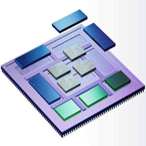
The solution is to take multiple dice, mount them on a common substrate, and present everything in a single package, which may be referred to as a “multi-die system.” In this case, the dice are commonly referred to as “chiplets.”
Multiple chiplets can be mounted on a common substrate and presented as an SiP (Source: Synopsys)
The reason I’m waffling on about all of this here is that I just had a very interesting chat with Manmeet Walia, who is Director of Product Marketing at Synopsys.
Manmeet informed me that, at the time of this writing, more than half of the aforementioned substrates are organic in nature, which we can take to mean small, special, high-density, printed circuit boards (PCBs). At the other end of the spectrum, we have silicon substrates, called “interposers,” with multiple layers of interconnect and through-silicon vias. Since these are implemented using silicon chip fabrication processes, albeit at a significantly higher technology node than the current state-of-the-art, we can currently achieve a reticle size of 2X that of today’s monolithic die, which equates to 1,700mm2 (~41mm x 41mm). Manmeet also says it won’t be long before we will be able to achieve 4X that of today’s monolithic die, which equates to 3,400mm2 (~58mm x 58mm). You can put a lot of dice on a 58mm x 58mm interposer!
Synopsys is, of course, a purveyor of the high-end electronic design automation (EDA) tools used to design chips, modules, boards, and systems. As part of this, they are establishing a leadership position on the chiplet front. I should perhaps mention that Manmeet was far too polite to say this out loud—it simply became apparent as our conversation progressed.
Manmeet told me that they’ve identified four main chiplet use cases, the connectivity of which may be referred to as die-to-die (D2D). The first is to simply scale things by mounting multiple homogeneous dice (think processors like CPUs, GPUs, NPUs, etc.) on the same substrate. The second is to take a design that you would ideally like to implement in the form of a humongous monolithic die and split it into two or more smaller chiplets.
The third scenario is based on the fact that input/output (I/O) functions like transceivers and memory interfaces typically don’t benefit from being implemented at the latest and greatest technology node. In this case, the best solution is to create the main die containing your “secret squirrel (logic) sauce” at the latest technology node, and to realize your high-speed interfaces as proven, risk-free chiplets implemented at an older process technology (some people refer to this as “N – 2 nodes”).
Last, but certainly not least, the fourth scenario involves disaggregating everything into heterogeneous dice implemented at the best nodes (in terms of cost, power, etc.) for those functions. For example, an RF die implemented using a 28nm process, analog-to-digital converters (ADCs) implemented in a 16nm process, and digital logic implemented in a 5nm process.
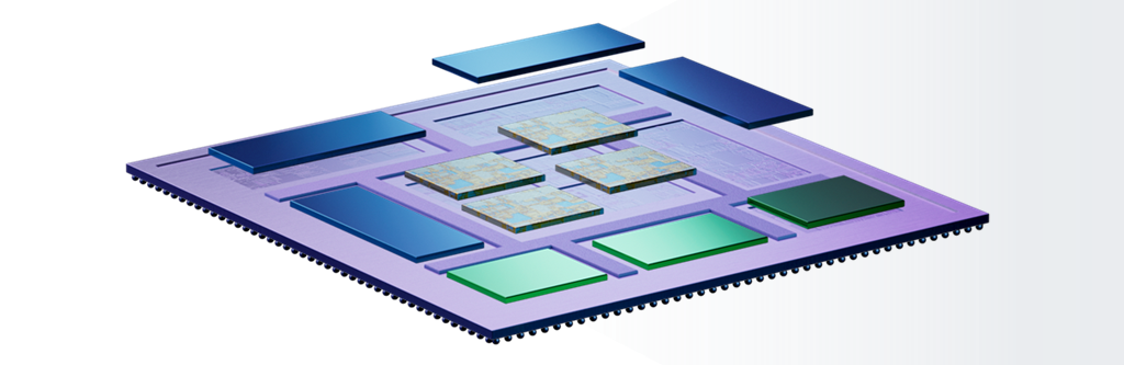
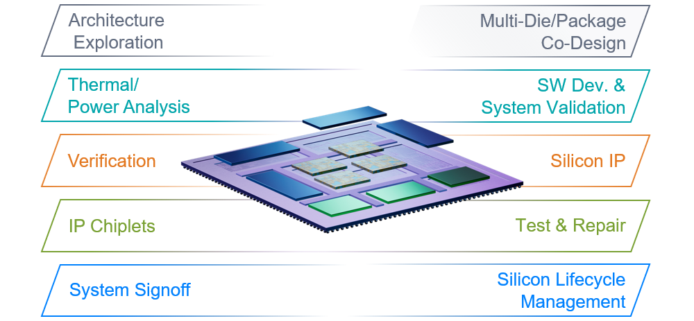 Synopsys multi-die system solution (Source: Synopsys)
To be honest, I’ve managed to touch on only a few of the myriad topics Manmeet and I discussed. There was so much more, such as universal chiplet interconnect express (UCIe), which is an open specification for a D2D interconnect between chiplets. Also, the fact that—as part of creating its UCIe IP—Synopsys is building testability and silicon life cycle management functionality into it. And then there’s the fact that Synopsys is partnering with network-on-chip (NoC) companies because you want NoCs in multiple chiplets to behave as a single super-NoC offering the highest possible bandwidths with the lowest possible latency. And of course… but no… that’s enough for today.
All I can say is my poor old noggin is now buzzing with chiplet-related ideas, notions, concepts, and conceptions. How about you? Do you have any thoughts you’d care to share on anything you’ve read here?


I am wondering how long before they realize that the crappy EDA that exists today is not even a good starting point.
Yes, I know that modules can be instantiated. Functionally a module and a chiplet are pretty much equivalent, I think.
Anyway , once you have cobbled a few of these thing-a-ma-jigs together it may pose the question, “Does it work in a functional way? And you have EDA to hep you. EDA has synthesis and static timing analysis, and you may claim simulation. Oh yes there may be a test bench or two laying around.
Once upon a time there was a project to build a micro processor based set of systems for applications for things like banking ATMs, super market checkouts — you know, all of the things we are surrounded by today.
So first there were 2 microprocessors dubbed UC0 and UC.5 to be designed. “UC zero” was in the same building where I worked. The design was done and sent to fab. And a TTL model was built, but it did not work. I was asked to lend a hand and we found the bug which as I recall was a wiring error, the design was fine.
But I realized there was no way to debug/trouble shoot a “system”. No control panel, other than power on/off so, Max this article brought back memories. Like a group of guys went bear hunting. One woke up early and went out alone. A short time later came running in the front door and out the back door. Slammed the back door shut and yelled “Skin this one, I’ll go find another”.
Love the bear hunting joke (I’ll be using this myself). Remember that I started my career working on a team designing CPUs for mainframes — we designed at the gate level using pencil and paper — and we dis timing analysis by adding gate, wire and load delays by hand — so by comparison I think today’s EDA tools are freaking awesome 🙂
Nah.
never gave a shit.
Something smells bad. Did you try to blow your nose but some of your brains came out of your misplaced anal orifice?
Chiplets are great for high value products. What about cost-sensitive devices?
One thing immediately comes to mind — The cost to fab a new chip. The only thing available off the shelf seems to be FPGAs. But there is a stigma(s): Too hard to design — Hooey. Too slow — That’s because the tool chain is only focused on synthesis. Well, duh, What is it that needs to be synthesized for an off the shelf module? There are typically hundreds of unused things … memory blocks especially that are not being used. They have already been synthesized, thank goodness, because synthesis wouldn’t know how. But the other part of the problem is that designers don’t know how to use them.
Q: “What about cost-sensitive devices?”
A: At the moment I would say “don’t use chiplets” LOL
Nice article. What I find really interesting is how manufacturers can mix chiplets made at different process nodes in the same overall packaging. That is a real innovation. Would be interested in knowing what design decisions are made in selecting chiplets vs SoCs… Apple chose SoCs for its M1/M2 processors, for example.
It is not the process node that matters, it is silicon on silicon so the thermal expansion is the same for the chip and Chiplet. I remember hearing the pipe dream of silicon on silicon at least 30 years ago.
You wrote “Apple chose SoCs for its M1/M2 processors, for example”…………
And a lot of critical clocking/timing just went away. Maybe it is not precisely SoC, the key is that structured interfaces wins versus native interfaces hands down.
Hope Max thinks about how this can be done with the crappy tool chain the rest of the world is stuck with.
“Hope Max thinks about how this can be done with the crappy tool chain the rest of the world is stuck with.”
I lay awake at night…. 🙂