

Do you think chiplets are tasty? I think I’ve just seen the future of chiplet-based design—well, one possible future—and it looks finger-licking good to me. Just to make sure we are all tap-dancing to the same skirl of the bagpipes, let’s start by setting the scene. For the purposes of these discussions, we will take the term integrated circuit (IC) to refer to a honking big ASIC, ASSP, SoC… that sort of thing.
A monolithic IC is one that is built on a single piece of semiconductor. The predominant semiconductor material is silicon, so we typically refer to a monolithic IC as being a silicon die or a silicon chip. Unfortunately, yield starts to fall off when the size of a die reaches around 25mm x 25mm = 626mm^2. The solution is to disaggregate (separate) the design into multiple dice, mount them on a common substrate, and present everything in a single package. The result may be referred to as a “multi-die system,” while the dice are commonly referred to as “chiplets” or “tiles.”
I’ve been seeing an upsurge of interest in chiplet-based technologies, as discussed in several recent columns (see Are You Ready for the Chiplet Age? and Chiplets for the Unwashed Masses and Is This the Ultimate Chiplet Interconnect Technology?).
Some companies have been using chiplets for several years now, but these tend to be outliers like Intel, who control all aspects of their design flow. The long-term goal for the rest of us is to establish standards that allow multiple vendors to create an ecosystem of plug-and-play chiplets that work seamlessly with each other. In the same way today’s designers combine soft intellectual property (IP) blocks to create a chip, tomorrow’s designers will combine chiplet IPs to create multi-die systems. We aren’t there yet, but what I’ve just seen is a huge step along the way.
Before we go there, I would first like to reintroduce you to a guy called Andreas Olofsson. Way back in the mists of time we used to call 2008, Andreas had an idea for the architecture for a high-performance low-power processing chip. He was so enthused by this idea that he left his job, retreated to his basement, and—fueled by coffee and sandwiches provided by his wife—singlehandedly designed and implemented a working prototype (you can read all about this in my column From RTL to GDSII in Just Six Weeks!). Andreas subsequently raised $900K in thirty days on a Kickstarter for “a supercomputer for everyone” called the Parallella. This $99 board subsequently shipped to 10,000+ customers.
The reason I mention all this here is to establish Andreas’s bona fides because I just discovered that his company, Adapteva, has transmogrified into a new entity called Zero ASIC, whose mission it is to develop a chiplet-based technology that will reduce both the time and cost required to develop an ASIC (IC) by 100X.
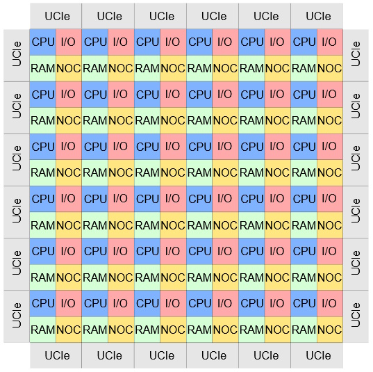
Now, this takes a little bit of effort to wrap one’s brain around, so we’ll take things step-by-step. Let’s start with eFabric, which is a network-on-chip (NoC)-based 3D active silicon interposer. (As opposed to a 2D passive silicon interposer that supports only point-to-point wiring, a 3D active silicon interposer supports active signal routing, switching, and buffering.)

Introducing eFabric and the chiplet library (Source: Zero ASIC)
Users can select between several eFabric sizes: 2×2 (small), 4×4 (large), and 8×8 (extra-large). The illustration above represents a 4×4 interposer. These eFabric silicon interposers are accompanied by a chiplet library, boasting functions like an Arm processor, a 32-bit RISC-V processor, a 64-bit RISC-V processor, SRAM, Non-Volatile Memory (NVM), a GPU, a machine learning (ML) accelerator, etc. This library will grow as Zero ASIC’s ecosystem partners add their chiplets into the portfolio.
One way to think about this is to consider the eFabric interposer to be like a breadboard into which we can plug the chiplets. Another approach is to visualize the eFabric interposer as being a sort of LEGO platform onto which we can plug LEGO chiplet bricks. Although each site shows only nine connection points in the illustration above, there would, of course, be thousands of connections per site on the real interposer.
But wait, there’s more. The illustration above shows only locations for the 3D chiplets (eBricks). In this case, die-to-die (D2D) communications are performed using a protocol called CLINK, which we might think of as “UCIe 3D.” Surrounding the locations for the 3D chiplets is a “ring” of locations for “2D I/O chiplets” (uBricks) that are used to interface to the outside world. These 2D uBricks connect to the 3D eBricks using standard UCIe interfaces (think “UCIe 2D”).
In the case of a 4×4 interposer, there will be 16 uBrick sites as illustrated below. These can be populated by ADC and DAC chiplets, PCIe and DDR chiplets, and… the list goes on.

3D eBricks and 2D uBricks (Source: Zero ASIC)
We all know that the number one rule in real estate may be summarized as “Location, Location, Location.” Well, in the case of multi-die systems, the rule in the future will be “Automation, Automation, Automation.” To illustrate this, Andreas has identified three enabling technologies as illustrated below.
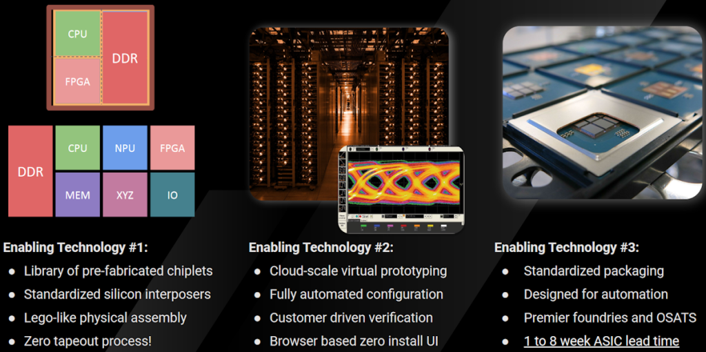
Three enabling technologies (Source: Zero ASIC)
We’ve already introduced Enabling Technology #1 in the form of standardized (2×2, 4×4, and 8×8) silicon interposers coupled with a library of prefabricated eBrick and Ubrick chiplets.
Enabling Technology #2 involves cloud-scale virtual prototyping using a tool called ChipMaker. This browser-based zero-install user interface (UI) allows you to select the size of your interposer and then drag and drop eBrick and Ubrick chiplets onto it. When you are ready, the system will automatically configure everything—including the system register map and the D2D interconnect—after which you can run cloud-based emulation and verification.
Last, but certainly not least, is Enabling Technology #3, which involves partnerships with premier foundries and OSATS in conjunction with standardized packaging solutions.
Although it won’t be possible from the get-go, Andreas is targeting ASIC lead times in the future as short as 1 to 8 weeks, to which all I can say is “Wowzers!”
Based on Andreas’s previous track record, coupled with the fact that Zero ASIC already has funding, I would bet my wife’s life savings that this company is destined for huge success. If I were wearing a younger man’s clothes, I would be pounding on Zero ASIC’s door asking for a job. But what about you? If you are interested in dipping your toes in the multi-die system waters, I see some very interesting positions open on Zero ASIC’s Career Opportunities page.
So, what say you? Do you have any thoughts you’d care to share with the rest of us regarding chiplets in general and/or Zero ASIC’s approach in particular?


Max! You haven’t told us how much it will cost! Can I also retreat to the basement and build something, or will I need to mortgage the house?
You pose a good question — I can’t believe I forgot to ask — I just emailed Andreas and asked — Max