

I love the smell of fresh chiplets in the morning, but I bet you hear that all the time these days. As you may recall, rather than creating a semiconductor device as a single humongous piece of silicon, the latest and greatest alternative is to take multiple dice, mount them on a common substrate, and present everything in a single package, which may be referred to as a “multi-die system.” In this case, the dice are commonly referred to as “chiplets” or “tiles.”
Like many things, this sounds easy if you say it quickly and loudly while gesticulating furiously (the way most English people attempt to communicate with non-English-speaking natives when travelling in foreign lands, such as France, for example).
Recently, I’ve been seeing a tremendous surge of interest and development in the chiplet domain, as evidenced by my two recent columns: Chiplets for the Unwashed Masses and Are You Ready for the Chiplet Age?
One aspect of all this to which I really hadn’t devoted too much (if any) thought was the problems associated with connecting the dice together.
There are a lot of different interconnect technologies around these days. As the old engineering joke has it: “Standards are great… everyone should have one.” The problem, of course, is that almost everyone does, so let’s briefly set the scene.
Let’s start with Peripheral Component Interconnect Express (PCIe), which is a high-speed serial computer expansion bus standard used for chip-to-chip (C2C) or board-to-board (B2B) communications. That is, an interconnect that exits one chip package and then traverses traces (possibly wires and cables) before entering another chip package.
PCIe has multiple layers. For our purposes here, however, we will take the simplistic view that there are only two: the physical layer at the bottom and the protocol layer that rides on top of the physical layer. The physical layer, which is closest to the serial link, is tasked with encoding and transmitting packets across the serial link and accepting and decoding packets received over the serial link. Meanwhile, the protocol layer defines and controls interactions across the link at a higher level of abstraction.
A somewhat related C2C/B2B standard is Compute Express Link (CXL), which is built on the PCIe physical and electrical interface, but which also offers cache-coherent protocols for maintaining cache coherency between device and system memory subsystems.
The problem is that the C2C versions of PCIe and CXL are too “top-heavy” for use in the die-to-die (D2D) interconnect realm (we can’t say “chiplet-to-chiplet (C2C)” because that would get confused with “chip-to-chip (C2C)”). In this case, two standards whose names invariably pop up in the conversation are Bunch of Wires (BoW) and Universal Chiplet Interconnect Express (UCIe). I can almost hear you muttering under your breath: “What are these little scamps, where did they come from, and—as great as they doubtless are—is there anything even better?” Happily, all these questions are about to be answered.
Have you heard of a company called Eliyan? This name seems to be on a lot of lips these days. Well, at least, on a lot of lips that are whispering in my ear. I can’t tell you how many people have said, “You need to talk with the folks at Eliyan,” so I determined to do so. In fact, I was just chatting with Ramin Farjadrad, who is Co-Founder and CEO, and Patrick Soheili, who is Co-Founder and Head of Business and Corporate Development at Eliyan. Ramin and Patrick certainly had a tale to tell, so sit down, make yourself comfortable, and we’ll begin…
Actually, there are so many layers to this onion that they made my head spin like a top, so I’m going to do my best to cut a long story short (which is opposite to the way I usually like to do things).
Way back in the mists of time we used to know as 2016 to 2017, Ramin was working at a company called Aquantia Corporation, which was a manufacturer of high-speed transceivers. Realizing that chiplets were going to become “a thing,” Ramin developed a short-reach serial D2D interface called AQLink, which was implemented in silicon and became a product used internally and by other companies. AQLink provided the physical layer—users could implement their protocol of choice on top of this layer.
Circa 2018 to 2019, the folks at the Open Compute Project (OCP) selected AQLink Unidirectional as their D2D physical layer open standard of choice (the AQLink Bidirectional patents were held back by Aquantia). AQLink Unidirectional is what became known as BoW (Bunch of Wires).
In 2019, Aquantia Corporation was acquired by Marvell Technology, which develops and produces semiconductors and related technology.
On a mission to overcome the hurdles in creating and deploying chiplets—Ramin and Patrick (and Syrus Ziai, who is VP of Engineering) co-founded Eliyan in 2021. At that time, they exclusively licensed AQLink Bidirectional from Marvell, and they immediately set about making it better and faster. The result is called NuLink (remember that name because we will be seeing more of it in a moment).
UCIe 1.0 was released in 2022. The UCIe standard includes both a physical layer and a protocol layer. The UCIe protocol layer is essentially the same as PCIe and/or CXL.
In April 2023, the folks at Eliyan taped out their NuLink silicon proof-of-concept (PoC) on a TSMC 5nm process. Remember that NuLink is the physical layer, which means you can run any protocol layer you want on top of it. To put this another way, NuLink is a superset of the UCIe protocol layer and the BoW physical layer.
All of which leads us to question, why would you want to run the UCIe protocol layer on top of the NuLink physical layer as opposed to running it on top of its own UCIe physical layer. Hmmm. Suppose I were to say, “Greater than 2x the bandwidth in less than half the area while consuming less than half the power”? Further, just to add a dollop of metaphorical cream on top of our allegorical cake, suppose I were to also say “And I haven’t even told you the interesting part yet”? Intrigued? Read on…
One of the problems with today’s chiplet-based systems is that they require some form of interposer. The most advanced packaging solutions employ silicon interposers. As seen in the image below, the D2D connections are either made in/on the silicon interposer (top) or on/in silicon bridges (bottom).
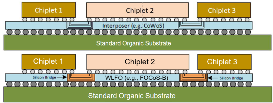
Multi-die systems using advanced packaging solutions (Source: Eliyan)
The only advantage of these solutions is high trace density, which enables high bandwidth at low power. By comparison, the disadvantages are manifold as follows:
- Interposer limits package size (maximum 3-4 reticles).
- Highest packaging cost and production cycle.
- Limited test coverage and lower yield.
- Limited reach and high thermal crosstalk.
- Poor power integrity.
- Long lead times/limited supply chain.
A more attractive solution in many ways is to mount the chiplets directly onto a standard organic substrate as shown below.
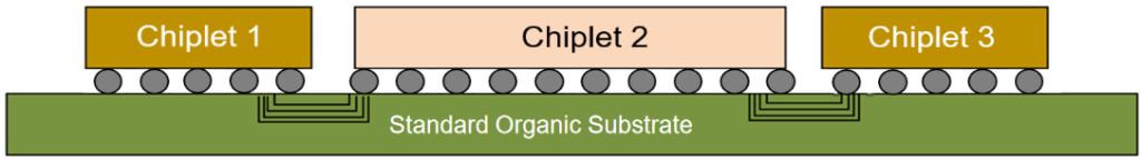
Multi-die systems using standard packaging solutions (Source: Eliyan)
In this case, the only disadvantage is low density traces, which limit bandwidth. By comparison, the advantages are numerous as follows:
- Enables large and complex systems in package (10-12 reticles).
- Low packaging cost and short production cycle.
- High test coverage and high yield.
- Long D2D reach and low thermal crosstalk.
- Good signal and power integrity.
- Widely available supply chain.
If only we could have the best of all worlds. Something that enables chiplet connectivity using standard packaging solutions while still receiving similar performance and power characteristics to those associated with advanced packaging solutions. “Good Golly, Miss Molly,” I cry, “this is where Eliyan’s NuLink technology leaps onto the center of the stage with a fanfare of sarrusophones (once heard, never forgotten).
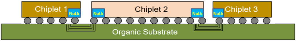
Multi-die systems using NuLink plus standard packaging (Source: Eliyan)
In this case, there really are no disadvantages or downsides, so all I can do is regale you with the advantages and upsides as follows:
- NuLink provides high bandwidth at low power.
- Enables large and complex systems in package (10-12 reticles).
- Low packaging cost and short production cycle.
- High test coverage and high yield.
- Long D2D reach and low thermal crosstalk.
- Good signal and power integrity.
- Widely available supply chain.
Of course, it’s easy for me to waffle on with wild claims, but what are we actually talking about in real numbers? I’m glad you asked. Let’s start with a solution based on a TSMC CoWoS silicon interposer, which offers 2.5Tbps/mm (that is, per mm along the edge of the chiplet) at <0.5pJ/bit with <2.0ns latency. Pretty impressive, eh? Well, yes, I suppose, were it not that Eliyan can achieve exactly the same values with NuLink and organic substrates.
With respect to the disadvantages and advantages presented above, what do we actually mean by “limited reach” in the case of the silicon interposer solutions and “long reach” in the case of the NuLink solution? How about 2mm for the former and 25mm for the latter? Take a moment to let that sink in.
There are so many facets to this that I could waffle on for hours, but I will restrain myself to noting that artificial intelligence (AI) computational processing for tasks like ChatGPT is currently running into (being limited by) the “memory wall.”
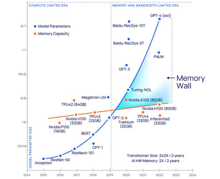
Artificial intelligence meets the memory wall (Source: Eliyan)
Suppose you are creating an AI ASIC. One part of the solution is to mount as much High Bandwidth Memory (HBM) as close to the main ASIC die as possible, where HBM involves stacks of DRAM memory dice. The problem is that if you are using a silicon interposer, the maximum reticle size you can achieve for the main die is ~600mm^2 (about 25 x 25mm) and the maximum reticle size you can achieve with a silicon interposer is 3-4X this, which limits what you can do as illustrated below (left).
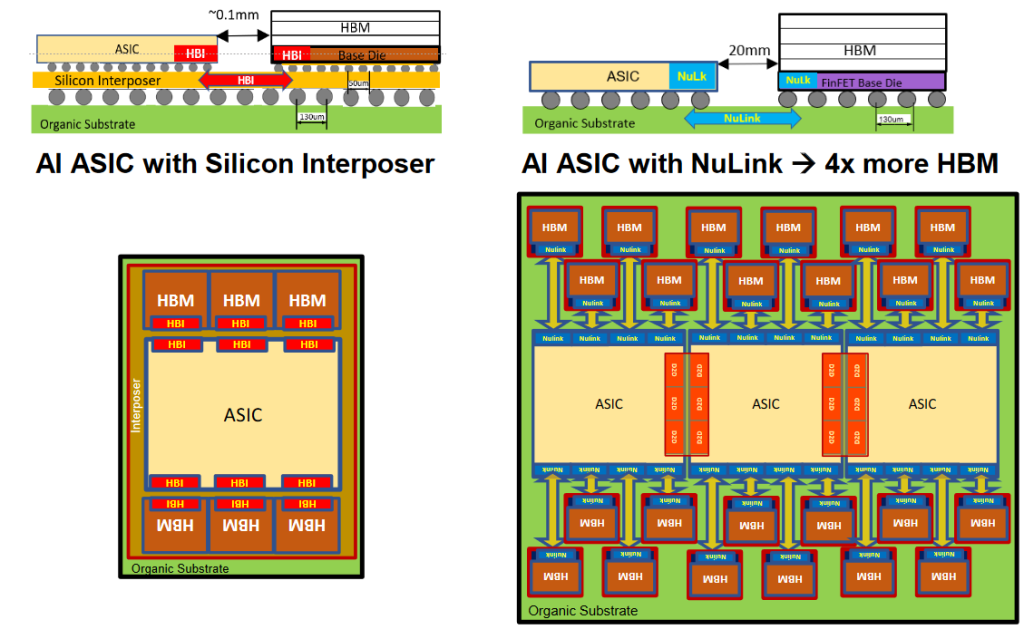
NuLink eliminates the memory wall for AI ASICs (Source: Eliyan)
By comparison, if you opt to use NuLink in conjunction with an organic substrate, the maximum reticle size you can achieve for your substrate is 10-12X the main die size, which allows you to add more of the main die and more HBM stacks as depicted above (right).
I for one am jolly impressed. But it’s not all about me (it should be, but it’s not). How about you? What do you think about all this?


