

I’m a simple man. We could stop this column here and call it a day, but mayhap you were expecting more. Oh well if you insist. As you are doubtless aware, there’s a lot of buzz about the forthcoming 2nm process node, but what does this term actually mean in the real world? Ah, therein lies the rub, as the Bard might say.
The term “process node” (a.k.a. “process technology,” “technology node,” or just “node”) refers to a specific semiconductor manufacturing process. As part of this, we include a number, like “The 90nm process node.” So, the real question is, “To what does this number refer?”
If I am talking to someone new to electronics, the way I typically describe this as “the size of the smallest structure that can be fabricated on the chip,” on the basis that—although this is a gross simplification—they are in no position to argue.
Actually, it is fair to say that the numbers associated with process node nomenclature did indeed refer to physical quantities in the dim and distant past, although what those quantities were depended on who you were talking to. Some people defined the node number as the minimum width of a track, some regarded it as being the length of the channel between the source and drain diffusion regions of a field-effect transistor (FET), and some… well, let’s just say that it quickly started to get complicated.
As an aside, it used to be common for people talking about earlier process nodes to describe those nodes in relation to the diameter of a human hair. For example, in the case of the first ASIC I designed in 1980, which was implemented at the 5µm technology node, you might see someone say something like “It contains structures 1/20th the diameter of a human hair.” The problem here (well, one of many problems) is that—as I noted in my book Bebop to the Boolean Boogie (An Unconventional Guide to Electronics)—human hairs range in thickness from around 0.07 mm to 0.1 mm. Since my wife (Gina the Gorgeous) is blond, it behooves me to note that a hair from a typical blond lady’s head is approximately 0.075 mm (three-quarters of one-tenth of a millimeter) in diameter, but we digress…
To be honest, the numbers associated with technology nodes did bear some relationship with reality up to and including the 32nm technology node, which was introduced circa 2009. For the purposes of simplicity, let’s assume that 32nm did indeed reflect the length of the channel between the source and drain diffusion regions of a field-effect transistor (FET). The problem is that this refers to a traditional Planar FET. But what about FinFETs, which are a cheval d’une couleur différente (“horse of a different color”), as it were?
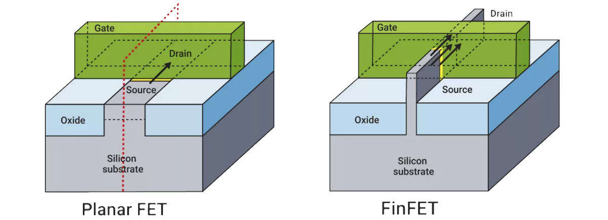
Planar FET vs. FinFET transistors (Source: Synopsys)
As opposed to having a channel that is planar (flat), a FinFET’s channel is presented in the form of a thin vertical fin. As we read on the What is a FinFET? page on the Synopsys website: “The gate is fully “wrapped” around the channel on three sides formed between the source and the drain. The greater surface area created between the gate and channel provides better control of the electric state and reduces leakage compared to planar FETs. Using FinFETs results in much better electrostatic control of the channel and thus better electrical characteristics than planar FETs.”
The first commercially available FinFET-based products were manufactured by Intel at the 22nm node. FinFETs became the dominant gate design with the 14nm, 10nm and 7nm process nodes. And, just for giggles and grins, it’s now common for FinFET transistors to contain several fins. These are arranged side by side and all covered by the same gate, acting electrically as one, thereby increasing both drive strength and performance.
But wait, there’s more, because there’s also the concept of gate-all-around (GAA) FETs in which the vertical fins in FinFETs are replaced with a stack of horizontal sheets. TSMC’s forthcoming 2nm node—which is expected to appear on the market circa 2025/2026—will feature GAA FETs.
As another aside, I hope the folks at TSMC are talking to the guys and gals at Flexciton with respect to using their AI-powered scheduling solution to Boost Semiconductor Fab Productivity by up to 20 Percent! I also hope the folks at TSMC are in communication with the chaps and chapesses at SandBox with respect to Accelerating and Reducing the Cost of Semiconductor Process Development. But, once again, we digress…
So, when we talk about a 5nm FinFET node or a 2nm GAA FET node, to what dimension are we referring? I don’t have a clue. To be honest, I think the node numbers of today are marketing-based, which means they are essentially meaningless. On the other hand, we could take the more charitable view that—even though a node number’s link to a physical dimension has become a little fuzzy around the edges—it’s still useful to think of things in these terms.
The reason I’m waffling on about all this here (yes, of course there’s a reason) is that I recently had the opportunity to chat with Shankar Krishnamoorthy, who is GM of the EDA Group at Synopsys.
Our discussion covered a lot of ground, but I think we can summarize it as follows. First, Shankar talked about some of the generational trends we are seeing with respect to the demands for dramatic increases in computational power. For example, the computational demands for generative artificial intelligence (GenAI) training are currently doubling approximately every 3.5 months! Then there’s the trend towards smart vehicles and autonomous driving. There are also the increased computation and bandwidth requirements associated with 5G and 6G communications. And there’s the whole digitization of industries as embodied by the Fourth Industrial Revolution (a.k.a. Industry 4.0).
There are various answers to these computational requirements. One solution is provided by innovations at the foundry level, such as the aforementioned 2nm technology node from TSMC. It is anticipated that moving from the 3nm node to the 2nm node will result in 10% to 15% speed increase, 10% to 15% area reduction, and 25% to 30% power improvements (give or take). In this case, in addition to all of Synopsys’s traditional Electronic Design Automation (EDA) design and verification tools, its technology computer-aided design (TCAD) is proving to be essential as engineers are figuring out how to get the next node operational, experimenting with different materials, different types of process structures, different recipes and so on (see also What Is TCAD and Why Is It Essential for the Semiconductor Industry?).
Another answer to the demand for increased computational capabilities is the increased use of artificial intelligence (AI) in the context of AI-enabled-and-enhanced EDA—as embodied by Synopsys.ai—which allows designers to differentiate their SoCs with progressively better power, performance, and area (PPA). AI is already prevalent with respect to optimization—give it a very large solution space coupled with reward functions and penalty functions, and AI is awesomely good at autonomously evaluating that solution space to determine the most optimal solutions. The folks at Synopsys are now moving to the next phase in the form of assistive and generative AI, which will include the ability to perform tasks like generating RTL, generating test benches, and generating verification collateral based on natural language and conversational interactions with the tools. Shankar says that we will soon be seeing some significant announcements from Synopsis in this domain (in the meantime, see 100+ AI-Designed SoCs and Counting!).
And, complementary to everything we’ve discussed thus far is the trend to use chiplet-based technologies to implement multi-die systems. Synopsys is riding the crest of this wave with respect to the EDA side of things (see also Are You Ready for the Chiplet Age?). I’ve personally been seeing a huge upsurge in the chiplet arena, as described in columns such as Chiplets for the Unwashed Masses, Is This the Ultimate Chiplet Interconnect Technology?, and Is This the Future of Chiplet-Based Design?
I don’t know about you, but I’m too young for all this excitement. I remember when the 1µm technology node was commercialized circa 1985 (this was the first process where CMOS became common, taking the baton from NMOS). At that time, everyone thought we were reaching the limits of what was possible. If anyone had said we would one day be working at 3nm, with 2nm on the way and 1nm beckoning us before the end of the decade, we would have patted them gently on the head while looking for some dried frog pills. What say you? Just how low do you think we can we go?


Max – as someone who began the journey at 5 micron lithography (or, for those over at Fairchild, 0.2 mils), and closed out his career with FinFETs, I will suggest the key silicon production factor in the medium term is energy per operation, which is flattening out. Retrofitting existing power-limited server facilities is going to get tougher. Expect to see a huge build-up of solar-based server farms (deserts, ocean) over the next decade.
You make a good point. With exascale computers currently coming online, each requiring its own 20MW power station, I can’t imagine where we will be or what we will be doing in 10 years time (but it will be interesting to see).
Server farms do not work with intermittent power sources.
Well — they do work, but not well LOL