Cadence is a pivotal leader in electronic design, building upon more than 30 years of computational software expertise. The company applies its underlying Intelligent System Design strategy to deliver software, hardware and IP that turn design concepts into reality.
Cadence Blog – Latest Posts

On-Demand Webinar About Adaptive Grid Refinement
Register only once to get access to all Cadence on-demand webinars. Unstructured meshing can be automated for much of the mesh generation process, saving significant engineering time and cost. However, controlling numerical errors resulting from the discrete mesh requires adaptation to the developing solution. Cadence CFD products Fidelity Pointwise and Fidelity Fine Marine provide mesh adaptation methods that use a continuous size field that gets updated as the solution progresses. As a result, adherence to the underlying CAD geometry is maintained, and mesh quality is ensured. Mesh adaptation has been successfully applied to industrial cases using a variety of flow solvers in the aerospace, turbomachinery, marine, and automotive sectors. In this webinar, we will explain the process in detail and show you various examples. Register today to learn how to generate the best mesh every time, automatically, with Adaptive Grid Refinement. Register only once to get access to all Cadence on-demand webinars.

Start Your Engines: Best Practices for Converting an Electrical Signal to a Logic Value with Mixed-Signal Modeling
Cadence Spectre AMS Designer is a high-performance mixed-signal simulation system. The ability to use multiple engines and drive from a variety of platforms enables you to "rev up" your mixed-signal design verification and take the checkered flag in the race to the market. The Start Your Engines! blog series will provide you with tips and insights to help you tune your simulation performance and accelerate down the road to productivity. Bonjour! In this post, I will explain how you can convert an electrical signal to a logic value using the Verilog-AMS standard language defined by Accellera. I will talk about three behavioral models and their comparison. You can then select the one you prefer for your application. First, let me draw the symbol for these models. The model is named E2L_conv and it has: One electrical input port, named e One logic output port named l This model has the following parameters: Parameter Name Description vdd=1.0 vdd supply voltage vthi=vdd/1.5 Upper threshold for conversion vtlo=vthi/2 Lower threshold for analog conversion vtol=vdd/100 Threshold voltage tolerance tr=10n Rise time ttol=tr/3 Time tolerance of crossing analogMaxStep=10p Analog solver maxstep The width between vthi and vtlo defines the hysteresis region. The E2Lconv module can be considered equivalent to an analog comparator. The only difference is that instead of an electrical output, it has a logic value output. The disciplines.vams file is included in each model to provide the necessary Verilog-AMS discipline definitions (electrical) and the definition of the voltage access function. Model 1: E2L model conversion operation for each timestep of an analog solver This model lets you perform an electrical-to-logic conversion at each analog step of the electrical solver. Inside the analog block, you generate a clock with the aevent variable. The aevent value is initiated at 1 and at each electrical solver step, it is multiplied by -1 . The variable aevent toggles iteratively between +1 and -1 . In the event solver, inside an always block, cross-event detection is used every time aevent values cross 0 . This is done via the always @( cross( aevent, 0, ttol, vtol )) function. This function generates events that force synchronisation between the electrical and digital solvers. In addition, in the analog context, the $bound_step function is used to specify the maximum time allowed between adjacent time points during simulation in the analog solver. By specifying an appropriate time steps value, you can force the simulator to track analog signals as closely as your model requires. When you set a small value for $bound_step , it will slowdown the the transient simulation because of the increased synchronization numbers between the analog and digital solver. After this, the digital driver of the logic value output is created. 1’b1 : Specifies that the electrical input is above the high threshold ( vthi ) 1’b0 : Specifies that the input signal is lower than or equal to the low threshold ( vtlo ) The lout output value with assign statement creates the logic driver in the envent solver. The testbench is an electrical source with a triangular waveform driving the electrical input. With SimVision MS, you can automatically create the schematic. It also annotates values in the schematic, as shown in the figure. The E2L_conv module described in Verilog-AMS is a mixed-signal model, so the instance is highlighted in blue. The resultant waveform plots are shown in the given figure. The waveform in red displays the electrical input, which is a triangular voltage. It is easy to see the vhti and vtlo threshold. The waveform in green displays the logic value output, with conversion operation. The signal transmission to 1’b1 happens when the V(e) value crosses the vthi Similarly, the signal transmission to 1’b0 happens when the V(e) value crosses the vtlo value. Model 2: E2L Model Conversion Based on Logic Events Controlled by Analog Input Reaching High and Low Thresholds The idea behind this model is to: Trigger the analog and event solver synchronization when the electrical input crosses either the vthi value on positive edge or when the vhlo thresold reaches the negative edge Perform an electrical-to-logic conversion This is done by two always blocks. The first always block is triggered by the V(e) value crossing the vthi theresold on a positive edge. The second always block detects when the V(e) value crosses the vtlo low voltage thereshold on a negative edge. The resultant waveform plots are as showin in the figure. The waveform in red displays the electrical input, which is a triangular voltage. It is easy to see the vhti and vtlo threshold The waveform in green displays the logic value output with conversion operation. The signal transmistion to 1’b1 happens when the V(e) value crosses the vthi Similarly, the signal transmission to 1’b0 happens when the V(e) value crosses the vtlo value. Model 3: E2L Model Conversion Based on Logic Events Controlled by Analog Input Reaching the High and Low Thresholds while Operating with Dynamic Supplies This module code reuses the ideas of model 2, but here, both high and low thresholds are dynamically computed based on the supply voltage v(vdd) measured on the testbench. This is done by introducing a new string parameter vddnode , which is an out-of-module reference node name for the testbench supply. In the module, analog context, the Verilog-AMS system function $analog_node_alias creates a mirror or an alias between this internal node vdd to the hierarchical node which is defined via a string reference tb.vdd . When the voltage V(vdd) changes, the high and low thresholds are updated. The resultant waveforms plots are as given in the figure. The waveform in yellow shows the V(vdd) supply voltage variation at 200ns from 1 volt to 2 volts. The waveform in red displays the electrical input, which is a triangular voltage. It is easy to see the vhti and vtlo threshold variation at 2 volts. The waveform in green displays the logic value conversion. The testbench simulation results show the E2L_conv operation when v(vdd)=1 volt in the time window 0s to 200ns , and when v(vdd)=2 , in the time window 200ns to 400ns . The vthi and vtho threshold values change according to the V(vdd) testbench supply values. Common Errors For model 1, 2, or 3 : Forgetting to define the cross or above tolerances (the time tolerance or the expression tolerance). It is important to define them because each simulator can have different definitions. For model 1: Defining a sampling period using the $bound_step value which is too small or too large versus the electrical signal activity. Model Comparison Model 1: It has a disadvantage of creating a large number of breakpoints in the electrical solver to provide the E2L conversion accuracy. The breakpoints must be optimized for each application. The AMS simulation can be very slow. Model 2: It has good usage, but only if you know the testbench vdd supply voltage in advance. This testbench supply voltage, vdd , should be constant to optimize the vthi and vtlo parameter values to your application requirements before launching the simulation. Model 3: Both the vthi and vtlo thresholds follow the testbench supply voltage variations. In addition, it triggers the electrical to logic conversion only when it is mandatory. All three models have an infinite analog input impedence. Conclusion Usually, a mixed-signal engineer would prefer model 3. This model has the advantage of adapting itself and smartly supplying values and input signal frequencies on different testbenches. It triggers the synchronization of both analog and event solvers only when this is needed. The behavioral electrical-to-logic concepts presented here can be reused for connect module creation with the Cadence Verilog-AMS or SystemVerilog-AMS compilers delivered inside Xcelium. This is very easy. You just need to replace module with connectmodule in the behavioral codes and create a .vams file for the connect rules. SimVision MS is very valuable for interactive debugging of such mixed-signal models, with Source Debugger, Design Browser, Waveform window, and Schematic Tracer. Hope you are now excited to try this feature out yourself! If you need more details, contact your Cadence Support team. Related Resources Product Manual Spectre AMS Designer and Xcelium Simulator Mixed-Signal User Guide Troubleshooting Information Spectre AMS Designer Spectre AMS Designer Product Page Blogs Start Your Engines: An Innovative and Efficient Approach to Debug Interface Elements with SimVision MS Start Your Engines: Win Le Mans with the SimVision Mixed-Signal Debug Option Start Your Engines: Mixed-Signal Modeling Methods for Converting an Electrical Signal to a Real Number Start Your Engines: Mixed-Signal Modeling Best Practices for Converting a Real Number Signal to Electrical For more information on Cadence circuit design products and services, visit www.cadence.com . About Start Your Engines The Start Your Engines series will bring you blog posts from several analog/mixed-signal subject matter experts on a variety of topics, such as introduction to the new features in AMS Designer, tips for enhanced working with existing features, and much more. To receive notifications about new blogs in this series, click Subscribe and submit your email ID in the Subscriptions box. - Andre Baguenier

System Analysis Knowledge Bytes: Summer's Here! Keep Cool by Coming to the Celsius Webinar!
The System Analysis Knowledge Bytes blog series explores the capabilities and potential of the System Analysis tools offered by Cadence®. In addition to providing insight into the useful features and enhancements in this area, this series aims to broadcast the views of different bloggers and experts who share their knowledge and experience on all things related to System Analysis. It was the summer of '07, a balmy 95-degree day where staying inside and playing on my gaming console was the best way to enjoy the day. Everything was great, I loaded my saved file, donned my helmet as the Master Chief, and was ready to take on the Covenant. A few hours in, and every gamer's worst nightmare happened; my system crashed. Two blinking red lights had signaled that my console had overheated. Perhaps if more thermal analysis had been completed, I wouldn't have lost 3 hours of game time; perhaps Celsius Thermal Solver could have saved that day. Thermal analysis is an ever-growing concern as power density and design complexity continue to increase, and product sizes continue to decrease. Celsius Thermal Solver is an analysis tool for predicting the effects of temperature distribution on the design of integrated circuits, packages, PCBs, and systems. Early detection and resolution of thermal compliance issues in the design cycle are critical for successful product development and prevents the potential delays and costly design fixes that otherwise might occur. Cadence will be hosting a free Celsius Thermal Solver training webinar for electrical and thermal co-simulation, where we will cover an Electronics Cooling (EC), formerly known as Computational Fluid Dynamic (CFD), workflow for PCB thermal analysis. What Is Celsius? Celsius Thermal Solver is the industry's first complete electrical-thermal co-simulation solution for the full hierarchy of electronic systems from ICs to physical enclosures. A common problem that is encountered in thermal and electrical testing and design is due to the relationship between heat and electrical resistance. Typically, as components warm up, their electrical resistances increase. And when electrical resistances of those components increase, so does their temperature as more electrical energy is converted to heat. Clearly, this is a self-feeding problem, and the solution requires convergence between the temperatures of the system and the electrical nuances of the system, and this convergence must be within both thermal and electrical tolerances for the system. For a static simulation, this can be fairly simple. But once we add in fans, heatsinks, enclosures, and other various components, the solution becomes a bit more complex. Why EC? An Electronics Cooling (EC) simulation will create a thermal model of the effects of airflow and a chassis by utilizing a computational fluid dynamics engine. In fact, this EC simulation is required when a system is accounting for the cooling effects of a fan and a chassis. The EC simulation will create a Heat Transfer Coefficient mapping file that defines the heat transfer coefficients for all the devices in the design, and this mapping file can be imported into Celsius Layered Structures so an accurate electrical and thermal co-simulation can be run that will include the cooling effects of the chassis, fans, and airflow. Webinar Agenda The free training webinar for Celsius will cover the following topics: The Three Celsius Thermal Solver Modules The Celsius EC/CFD Workflow for PCB Thermal Analysis Simplified EC/CFD Model Generation Adding Heat Sinks Defining a Chassis, Fan, and Openings Generate an HTC Mapping File Running a Complete Simulation Date and Time Thursday, June 15, 2023 07:00 PDT San Jose / 10:00 EDT New York / 15:00 BST London / 16:00 CEST Berlin / 17:00 IDT Jerusalem / 19:30 IST Bangalore / 22:00 CST Beijing How to Register To register for the Celsius Thermal Solver: Electrical and Thermal Co-Simulation webinar, use the link found HERE and sign in with your Cadence Support account (email ID and password) to log in to the Learning and Support System. Then select " Enroll " to register for the session. Once registered, you'll receive a confirmation email containing all login details. If you don't have a Cadence Support account, go to Registration Help , or Register Now and complete the requested information. I hope to see you all there! Related Resources Datasheet Datasheet link here For more information on Cadence Sigrity and Systems Analysis products and services, visit www.cadence.com . Contact Us For any questions, feedback, or new content development ideas, write to system_analysis_blogs@cadence.com .

Using AI-Driven Verification to Improve Productivity in Electronic Design
Join us for the latest The Future of Electronics podcast! In this episode, we meet Matt Graham, director of Product Engineering, to talk about how Cadence is leveraging the power of AI to boost productivity and improve the efficiency of electronic design. With traditional verification methods being time-consuming, labor-intensive, and costly, Cadence is revolutionizing the field with AI-driven verification, providing faster, more accurate, and more comprehensive verification results. With automated self-driving cars and driver-assist features, the chips powering these systems must be safe and reliable. Join us for an insightful conversation about the complex world of chip design and how AI-driven verification is shaping the future of electronic design. Episode three of “The Future of Electronics – Designed with Cadence” podcast is available now on Spotify —don't forget to subscribe! Check our Designed with Cadence page and YouTube channel for more videos on how Cadence is helping build the future.

How Stringent Are the Aerodynamic Testing Regulations in Formula One Racing?
Get ready to hold on to the edge of your seats, fellow F1 fans! The upcoming Formula One season promises to be an exhilarating and heart-stopping spectacle. The Fédération Internationale de l'Automobile (FIA) committee has proposed an array of new design regulations that will push the limits of driver and vehicle safety. Teams will be given the opportunity to get creative within the restrictions, with upgrades to floor flexing, side-view mirrors, fuel cooling, roll hoop design, and more. With new testing restrictions in place to ensure compliance with FIA regulations, the competition is bound to be fierce. The Miami Grand Prix witnessed Max Verstappen take the first position, and now, McLaren is gearing up for the Emilia Romagna Grand Prix at the Autodromo Enzo e Dino Ferrari. While the race dates have been postponed due to heavy floods, we can still look forward to an unforgettable season of high-speed thrills and spills! What Are the Aerodynamic Testing Restrictions (ATR) for Formula One Racing? Until 2008, there were no restrictions on aerodynamic testing hours in F1. Some top teams, such as BMW Sauber, Honda, Williams, and Toyota, were investing millions of dollars into operating wind tunnels. These teams also used computational fluid dynamics (CFD) tools in their design validation cycle. At that time, BMW Sauber used the Albert 3 supercomputers with 4000 Intel cores . Racing authorities soon realized that deploying testing restrictions was necessary to avoid the unfair advantage for a few teams that could invest their finances into 24/7 wind tunnel testing and multi-core CFD simulations. In 2009, as a step towards curbing the testing hours, the Formula One Teams Association (FOTA) signed a resource restriction agreement, and today, the teams at Formula One have to follow these testing restrictions. Failure to comply with these regulations will invite a penalty. The 3D representation (physical or digital) of the vehicle design is referred to as Restricted Aerodynamic Test Geometry (RATG) , and teams are allotted 6 Aerodynamic Testing Periods (ATP) per year. The first testing period is at the end of week 9. The 2nd, 3rd, and 5th testing period lasts eight weeks each. Ten weeks are allotted for the 4th testing period, including the 14-day summer factory shutdown. The last or 6th testing period ends by the 31st of December . Teams must follow the wind tunnel and CFD testing restrictions to validate their vehicle’s aerodynamic performance. What Are the Restrictions Imposed on Wind Tunnel Testing in Formula One Racing? The wind tunnel to be used for aerodynamic testing has to be nominated by the team to the FIA, and only one wind tunnel can be used in a 12-month period . According to FIA, in restricted wind tunnel testing (RWTT) , a single run commences when airspeed rises above 5m/s and ends when it falls below 5m/s. Once air speed is above 5m/s the RATG must remain fixed until below 1m/s . Changes to RTAG are permitted between runs of RWTT, and only two occupancy shifts are allowed per calendar day. Other sets of RWTT restrictions include that the RATG must be less than 60 percent of full-size vehicles , the wind tunnel speed should not exceed 50m/s, only two models can be tested in 24 hours, and creating curved flow conditions for testing is restricted. What Are the Restrictions on CFD Simulations in Formula One Racing? Restricted CFD simulations (RCFD) include all three steps in a CFD workflow, i.e., preprocessing, solving, and post-processing. CFD simulations conducted at scales other than 1:1 or using non-gaseous are also RCFD solutions that provide insight into gaseous flows on the full-size F1 vehicle. Machine learning, artificial intelligence, and deep learning-based simulation results are allowed only during the post-processing stage of RCFD simulatio n. Moreover, the team’s compute resources must contain a set of homogeneous processing units nominated to the FIA. The 2022 budget for each team was 6 million Allocation Unit hours (AUh) . An AUh is equivalent to a core hour on a physical CPU core. Non-RCFD can be done for optimizing CFD methodology but must be on RATG that was simulated 30+ months ago . How Can Cadence CFD Solutions Revolutionize Racing Car Design Time? Cadence recent investment in Fidelity Cascade Technologies brings high-fidelity CFD solvers to the table, including LES turbulence modeling with GPU acceleration for high throughput, and can do wonders in pushing the limits in racing and F1. The table below presents a variety of system-level high-fidelity multi-physics simulations that can be completed in just a few hours using the GPU-resident Fidelity CharLES solver. These simulations can take days and weeks on the CPU, making them impractical for design purposes. GPU-acceleration and GPU-resident solvers allow the exploration of complex design spaces with unprecedented speed and accuracy. In fact, it is fundamentally changing the game. The graph below compares the simulation throughput of an ensemble of Fidelity multi-physics LES performed on CPU and GPU. For a given investment in compute, based on AWS pricing of CPU and GPU nodes, the NVIDIA GPUs deliver nearly nine times the throughput of the CPU. Currently, F1 regulates CFD use because it significantly improves the performance of the cars. For example, while addressing the stability challenge of cars in F1, they used 7500 CFD simulations and 16.5 million core hours of compute to introduce new aerodynamic regulations, thereby improving the downforce from 55% to 86% . F1 does not currently allow GPU acceleration of the solvers due to compliance with the AUh definition. These strict limits confine the types of CFD simulation performed. While F1 is not benefiting from GPU, this transformation already impacts other areas of racing, commercial automotive, and many other industries. Are you looking for a simulation suite that can help you reduce racing car design time? Cadence Fidelity CFD solutions might be just what you need, with or without GPU acceleration. If you want to explore and get hands-on with the new Cadence Fidelity CFD tools, you can request a demo today!

How Do You Solve a Problem Like Clock Tree Synthesis?
Clocks for measuring time are one of the oldest inventions. Timekeeping has advanced from sundials and hourglasses to the world’s most accurate clock, which happens to be in the United States. The National Institute of Technology built the clock, and it is reportedly so precise that it does not lose even a second over the entire age of the universe. Just as clocks are central to modern life, clock trees are central to digital design implementation. Synthesizing and optimizing clock trees is one of the biggest challenges in implementation. If not optimized, the clock network can dissipate up to 30% -40% of your design’s power and contribute to missing your design’s PPA targets. The Clock Concurrent Optimization (CCOpt) technology in Innovus merges timing optimization with clock tree synthesis, thus converging your PPA requirements faster. The CCOpt tool also leverages useful skew for timing optimization and includes a visual debugger that helps you pinpoint violations. This video on the Cadence Support site illustrates how to use the clock tree debugger . To learn more about how to use the CCOpt tool to achieve the best results, register for the course Innovus Clock Concurrent Optimization with Stylus Common UI . After completing the course, you will be able to: Implement the clock tree using CCOpt technology using the generated constraints Specify clock properties to customize the clock tree, including: Defining route types, CTS cells, stop and ignore pins Modifying source latency settings in hierarchical implementation to meet timing at the block level Analyze and debug the tree using the information in the log file Analyze the QoR of the generated tree Assess how CCOpt analyzes chains between register stages, and Recognize when CCOpt uses slack in chains to meet timing Review the log file and determine how the worst chain analysis report can provide additional information about why the timing could not be met. Run the Clock Tree Debugger in trial and cluster modes of CCOpt to determine causes for unmet clock targets. Evaluate the advantages and disadvantages of various clock structures Implement a flexible H-tree After completing the course, you can take the exam , and when you pass the exam, you will receive a badge that you can display on social media. Happy Learning! Vinita

Cadence Welcomes Pulsic, Ltd
Cadence welcomes Pulsic, Ltd., a longtime provider of production-proven technology for floorplanning, placement, and routing of custom ICs. Pulsic technologists have worked with leading semiconductor companies for almost 25 years to provide innovative analog, custom design, and memory layout and routing solutions. These technologists will also bring a wealth of knowledge about using AI to solve challenging advanced-node problems using better planning techniques and virtual prototyping. The addition of Pulsic further strengthens Cadence's Virtuoso Studio commitment to using AI to facilitate our many customers as they push through the traditionally manual tasks of custom design and enter new realms of design possibility via automation and innovation. Pulsic’s technology line includes its Unity Planning and Implementation Solutions, which provide comprehensive signal planning, placement, and routing capabilities. Additionally, they offer Animate Preview, which provides designers with quick, easy, and accurate physical information about your analog circuit while you develop your schematic, reducing the overall turnaround time for your design. We welcome the entire Pulsic Ltd team to Cadence.

Meet the 2022 Latinx Students in Technology Scholarship Recipients
We are thrilled to congratulate the recipients of the Latinx Students in Technology program by showcasing their outstanding achievements and inspirational stories with this fifth and final installment of the Diversity in Technology Scholarship blog series. These highly accomplished awardees are pursuing technical degrees and were selected to receive a scholarship based on their impressive academic records, work in the community, leadership potential, and recommendations from professors. Get to know these spectacular students by hearing from them directly as they dive into their personal experiences, post-graduation goals, and what drives them to shape the future of technology. https://youtu.be/WQxnQuBKJko Amelia Churchill , Case Western Reserve University “I was inspired to study computer science after I created my first website with HTML, CSS, and Javascript when I was about nine years old. I loved that I was able to have full creative freedom over my website. Ever since then, I've always known I would pursue technology! My greatest piece of advice is to truly believe in yourself, and know that you have control over your future. ” Ana Luisa Veroneze Solorzano , Northeastern University “I have always liked to challenge myself by learning new things. Computer science and engineering allow me to work on real-world problems to develop new skills and techniques that will be used for scientific advancement. I believe that the moment I understood that my soft skills give me a unique comprehension to solve technical problems, I recognized I could make a great impact in the world.” Cristhian Alexis Roman Vicharra , Texas A&M University “As a recipient of the Latinx Students in Technology Scholarship, my motivation to share my experience with young students in my home country has increased. Also, my commitment to research and contribution to the technology field has gotten even stronger. Thus, I am committed to participating in conferences around South America and sharing my current research and experience.” Davi Valerio de Queiroz Rodrigues , Texas Tech University "I developed a great interest in researching RF and microwave sensing technologies and their various applications because I have always had a lot curiosity about how wireless technologies work. After graduation, I plan to pursue a career in either academia or industry as a researcher, and I am grateful for the Cadence Diversity in Technology Scholarship, which will help me to continue to work on my PhD dissertation." Jorge Quesada , Georgia Institute of Technology “After I graduate, I want to become a research scientist who can contribute to the development of neurotechnologies. I am very interested in how learning and intelligence arose in humans and the way we can implement it artificially .” Nubia Correa , Stanford University “Given that there are not a lot of people of color pursuing engineering-related degrees, I want to encourage students to teach what they learn to their communities, whether it's STEM-related concepts or general life lessons that the field has given you. It's a service for the passion you want to leave for the next generation to expand further and develop.” Omar Barrera , University of Texas at Austin “My advice to future students is to become involved in student organizations, professors’ office or coffee hours, and other similar department-run events. Always be willing to share knowledge and lend a hand first on matters where you have something to offer. Good things and opportunities have a way of finding those who give back.” Patricia Garcia , University of Southern California “I am aware that my goals will remain dreams if I do not continue to persevere. Therefore, I am committed to working hard in school and searching for ways to make my dream of obtaining a STEM degree a reality. The Cadence Diversity in Technology Scholarship has offered just that! I've been able to work on my startup and create a meaningful impact in my college community as I don't have to worry about my graduate finances.” Cadence is proud to support students from underrepresented communities in technology and thanks everyone who submitted applications this year. We hope to continue reaching STEM students from underrepresented groups with our upcoming scholarships. Congratulations to the talented individuals who were selected for everything they have accomplished thus far. We appreciate them sharing how these programs have impacted their studies and are excited to see where their passions take them next. Learn more about the Diversity in Technology Scholarship and say hello to other recipients from 2022 .
Chalk Talks Featuring Cadence

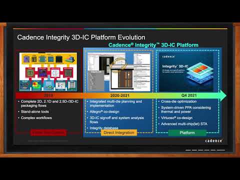
Faster, More Predictable Path to Multi-Chiplet Design Closure
The challenges for 3D IC design are greater than standard chip design - but they are not insurmountable. In this episode of Chalk Talk, Amelia Dalton chats with Vinay Patwardhan from Cadence Design Systems about the variety of challenges faced by 3D IC designers today and how Cadence’s integrated, high-capacity Integrity 3D IC Platform, with its 3D design planning and implementation cockpit, flow manager and co-design capabilities will not only help you with your next 3D IC design.

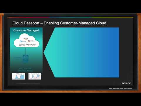
Enabling Digital Transformation in Electronic Design with Cadence Cloud
With increasing design sizes, complexity of advanced nodes, and faster time to market requirements - design teams are looking for scalability, simplicity, flexibility and agility. In today’s Chalk Talk, Amelia Dalton chats with Mahesh Turaga about the details of Cadence’s end to end cloud portfolio, how you can extend your on-prem environment with the push of a button with Cadence’s new hybrid cloud and Cadence’s Cloud solutions you can help you from design creation to systems design and more.

Machine-Learning Optimized Chip Design -- Cadence Design Systems
New applications and technology are driving demand for even more compute and functionality in the devices we use every day. System on chip (SoC) designs are quickly migrating to new process nodes, and rapidly growing in size and complexity. In this episode of Chalk Talk, Amelia Dalton chats with Rod Metcalfe about how machine learning combined with distributed computing offers new capabilities to automate and scale RTL to GDS chip implementation flows, enabling design teams to support more, and increasingly complex, SoC projects.

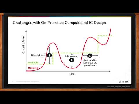
Cloud Computing for Electronic Design (Are We There Yet?)
When your project is at crunch time, a shortage of server capacity can bring your schedule to a crawl. But, the rest of the year, having a bunch of extra servers sitting around idle can be extremely expensive. Cloud-based EDA lets you have exactly the compute resources you need, when you need them. In this episode of Chalk Talk, Amelia Dalton chats with Craig Johnson of Cadence Design Systems about Cadence’s cloud-based EDA solutions.
Featured Content from Cadence
featured video

Find Out How The Best Custom Design Tools Just Got Better
The analog design world we know is evolving. And so is Cadence Virtuoso technology. Learn how the best analog tools just got better to help you keep pace with your challenging design issues. The AI-powered Virtuoso Studio custom design solution provides innovative features, reimagined infrastructure for unrivaled productivity, generative AI for design migration, and new levels of integration that stretch beyond classic design boundaries.
featured video

Automate PCB P&R Tasks for Designs in Minutes
Discover how to get a dramatic reduction in design turnaround time by automating your placement, power plane generation, and critical net routing with Cadence® Allegro® X AI technology. Built on and accessed through the Allegro X Design Platform, Allegro X AI reduces P&R tasks from days to minutes with equivalent or higher quality compared with manually designed boards.
featured video

How to Harness the Massive Amounts of Design Data Generated with Every Project
Long gone are the days where engineers imported text-based reports into spreadsheets and sorted the columns to extract useful information. Introducing the Cadence Joint Enterprise Data and AI (JedAI) platform created from the ground up for EDA data such as waveforms, workflows, RTL netlists, and more. Using Cadence JedAI, engineering teams can visualize the data and trends and implement practical design strategies across the entire SoC design for improved productivity and quality of results.
featured video

Get Ready to Accelerate Productivity and Time to Market with Overnight Chip-Level Signoff Closure
Is design closure taking too long? Introducing the Cadence Certus Closure Solution, a revolutionary new tool that optimizes and delivers overnight design closure for both the chip and subsystem. Learn how the solution supports the largest chip design projects with unlimited capacity while substantially improving productivity by up to 10X.