


In the microelectronics industry, the term “semiconductor fabrication plant” (a.k.a. “semiconductor fab”; sometimes called a “foundry”) is a factory for semiconductor device fabrication. In layman’s terms, this is where they build the silicon chips that power our modern world. Even a small fab can easily cost $1 billion. Spending $3 to $5 billion is not uncommon, and you can splash a lot more cash than this without straining yourself if you are so inclined.
The CHIPS and Science Act, which was signed into law by President Biden on 9 August 2022, includes ~$52 billion for American semiconductor research, development, manufacturing, and workforce development. As a result, several companies have unveiled plans for new US-based fabs, but it will take years for these plants to come online. In the meantime, legacy fabs will have to do the best they can to “hold the line.” And, even when the new fabs do become available, the world’s insatiable demand for semiconductors means their legacy cousins will continue to have a part to play for years (perhaps decades) to come.
Not surprisingly, since so much money is involved, the folks who own and operate fabs are keen to optimize their productivity. As a result, those who don the undergarments of authority and stride the corridors of power are going to be very interested to hear about a company called Flexciton, whose mission in life it is to streamline the incredibly complex problem of wafer fab scheduling.
I was just chatting with Flexciton’s Co-Founder and CEO, Jamie Potter, who informs me that, by employing Flexciton’s solution, even state-of-the-art fabs can experience a 3% to 10% boost in productivity, while legacy fabs can expect to see a 10% to 20% productivity improvement. O-M-Goodness gracious me! All I can say is that if I were overseeing such a fab, I would immediately devour the remainder of this column, after which I would start pounding on Flexciton’s door pleading to become a customer.
Intrigued? Read on…
Just to set the scene, let’s remind ourselves that, in electronics circles, the term “wafer” refers to a thin slice of semiconductor, such as crystalline silicon (c-Si), which serves as the substrate (base) in which, and on which, microelectronic devices and structures are built. Standard wafer diameters at the time of this writing are 200mm (which may be referred to as “8 inch”) and 300mm (which may be referred to as “12 inch”).
These wafers undergo many microfabrication processes, such as doping, ion implantation, etching, thin-film deposition of various materials, and photolithographic patterning. Finally, the individual microcircuits are separated by wafer dicing, after which they are packaged as integrated circuits. A modern process may involve anywhere between 1,000 and 2,000 individual process steps from when it is presented to the “input end” of the fab to when it eventually re-emerges back into the light of day from the “output end” of the fab.
How long do you think this entire process takes? If you’d asked me before I talked to Jamie, I might have hazarded a guess at one to two days. You can only imagine my surprise to discover that it takes a minimum of one month with the fabs Flexciton is working with. And, in fact, it can take up to nine months for the more advanced and complex processes. Wow!
Tortuous Terminology
Companies that own their own foundries, which are used to create devices to satisfy their own designs, are known as “Integrated Device Manufacturers (IDMs).” By comparison, companies that farm out the manufacturing of their designs to foundries owned by other companies are called “fabless semiconductor companies,” while foundries that build devices only for other companies are known as “pure-play semiconductor foundries.”
When you hear the terms “fab” and “line,” what exactly comes into your mind? Many people visualize a large factory containing a long line of machines. As part of this, they also envisage a linear process in which a wafer is passed from one machine to the next down the line. Ah, if only things were so simple.
This can be a bit tricky to wrap your brain around, so let’s take things step by step. First, what do we mean by “fab”? You might be thinking of something like a factory or facility. In fact, such an entity will typically feature multiple clean rooms, which is where the semiconductor fabrication takes place. Each clean room will handle only 200mm or 300mm wafers, and each will be dedicated to a particular process, like CMOS, or Bipolar, or MRAM. Furthermore, more advanced process nodes like 7nm, 5nm, 3nm and so on will require more expensive machines, so one CMOS clean room may handle only a small range of CMOS process nodes, for example. On this basis, we might say that the term “fab” is synonymous with “clean room,” while acknowledging that others may think of things differently.
Myriad machines are involved in semiconductor production lines. Some of these machines perform only a single operation, while others undertake multiple tasks. An example of the latter is the Endura Clover from Applied Materials, which I introduced in my Metrology Maketh the Man (and Woman, and Silicon Chip) column.
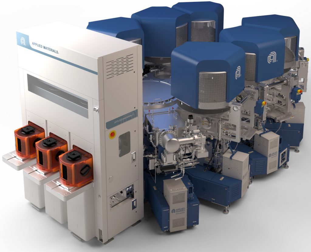
Applied Materials’ Endura Clover mainframe (gray) with cassettes (orange) and a collection of
wafer processing chambers (blue) (Source: Applied Materials, Inc.)
In this case, the entire machine is known as a “mainframe.” On the front we see three removable “cassettes” in orange. Each of these cassettes can hold 25 wafers, which are maintained in a nitrogen atmosphere to prevent oxidization. Some mainframes can handle only one cassette, while others can handle six or more.
Each mainframe has several processing chambers associated with it (six, in this example), where each chamber performs a specific task, like depositing an oxide layer, depositing a layer of resist, etching the oxide layer, and so forth. There’s a “robot” in the center of the chambers. This robot can remove a wafer from one of the cassettes and feed it into one of the chambers; remove a wafer from one chamber and feed it into another; and eventually return the wafer to the cassette, where all these movements take place in a nitrogen atmosphere or under vacuum.
It probably goes without saying that this equipment is extremely expensive. Prices for the most common pieces of equipment for the processing of 300mm wafers can range from $700,000 to upwards of $4,000,000 each. And some pieces of equipment (e.g., extreme ultraviolet EUV scanners) can cost upwards of $300,000,000 apiece.
The Problem
Earlier, we said that a modern semiconductor fabrication process may involve anywhere between 1,000 and 2,000 individual process steps. This doesn’t imply there are 2,000 unique machines (by “machines,” I find it helps to think “chambers in mainframes”). In fact, there are around 50 different types of machines; these different types may be represented in different quantities; and a typical clean room may boast hundreds of the little rascals.
How are the cassettes transported from mainframe to mainframe? I’m glad you asked. There are three main approaches. In legacy fabs, it’s often people who are physically moving the cassettes and loading them onto the mainframes. In many modern fabs, an automated material handling system (AMHS) in the form of a ceiling-mounted conveyor system transports the cassettes from mainframe to mainframe.
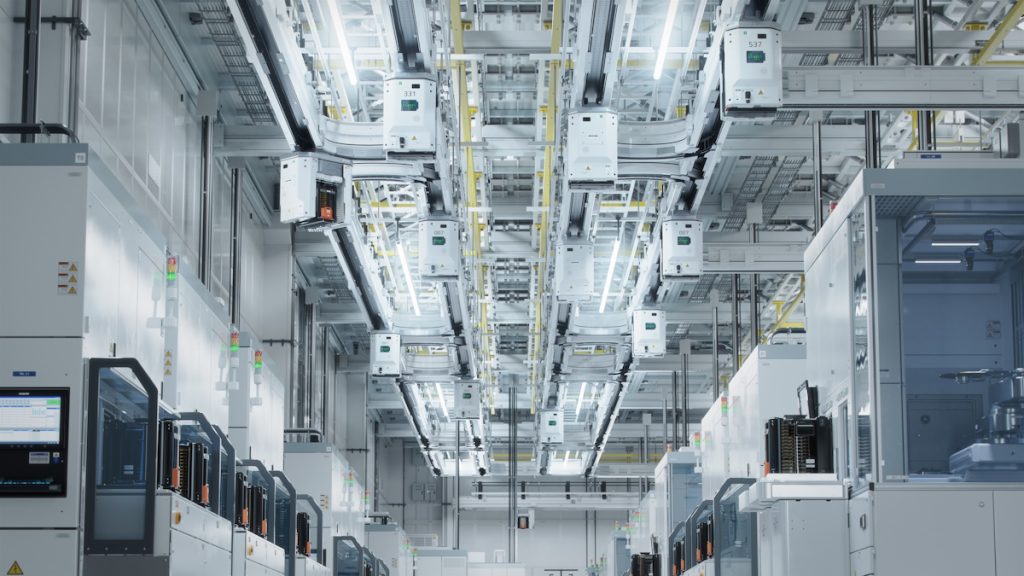
Ceiling-mounted conveyor system transporting cassettes from mainframe to mainframe (Source: Shutterstock)
If it isn’t possible to add a ceiling-mounted conveyor system to an older facility, ground-based robots may be used to convey the cassettes from mainframe to mainframe. In some cases, a combination of a ceiling-mounted conveyor and ground-based robots may be employed.
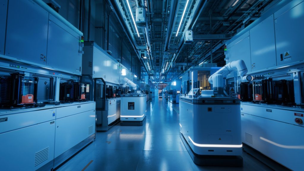
Ground-based robots and ceiling-mounted conveyor transporting cassettes from mainframe to mainframe
(Source: Shutterstock)
At the time of this writing, there are about 500 companies that own about 1,000 fabs around the world. This tends to be exponentially skewed, with many companies owning only one fab, while a few companies own many fabs.
When it comes to scheduling, there are so many problems that I don’t know where to start. For example, the wafers don’t follow a linear path from one mainframe to another. Instead, they go round and round in circles, reusing the same mainframes (sometimes the same sequence of mainframes) multiple times, often “bumping” into each other at certain tools.
Also, wafers typically spend different amounts of time in each chamber in a mainframe. If we assume a mainframe that can support a single cassette and that has six chambers, and we also assume that each wafer must pass through all six chambers, then the bottleneck will—obviously—be the slowest chamber. In such a case, it may be that two of the chambers are dedicated to perform the same function.
Another possibility is that one type of wafer requires the services only of chambers 1, 3, and 5, while another type of wafer requires the services only of chambers 2, 4, and 6. If the mainframe can support multiple cassettes, then all the chambers can be employed at the same time.
Let’s ramp things up a bit. Remember that each fab (clean room) may be handling hundreds of different types of wafers for different customers with different due dates. Existing production runs are constantly ending, new production runs are constantly starting, and priorities are constantly changing. Suffice it to say that scheduling all the wafer types in all the chambers to obtain maximum utilization of all the machines is a non-trivial task.
But wait, there’s more, because a semiconductor fab is an exceptionally dynamic environment. Suppose you oversee scheduling and you’ve just got things running smoothly when a favored customer places a large, high-priority order. And, just to increase the fun and frivolity, suppose that as soon as you’ve wrapped your brain around this conundrum, one or more chambers (or mainframes) in your clean room decide to take a break for some unscheduled maintenance.
The clock is ticking… What are you going to do? Who are you going to call?
The Solution
In a crunchy nutshell, the solution is to reach out to the folks at Flexciton because this is their very reason for being. Over the past few years, they’ve developed artificial intelligence (AI)-based scheduling software that is targeted at semiconductor fabrication facilities boasting multiple clean rooms, each of which contains hundreds of mainframes, each of which offers multiple chambers.
The first step is to tell the Flexciton software how many clean rooms there are. Also, how many mainframes (and other machines) there are in each clean room. Also, how many cassettes each mainframe can handle. Also, how many chambers (and their functions) are associated with each mainframe. Also… you get the idea.
You also need to inform the software about all the jobs you wish to control: “Customer A wants 10,000 wafers implemented using Process X with a due date of Y,” type thing.
The great thing is that you don’t have to specify any rules to the AI, just your objectives. For example, your main objective might be to generally maximize the capacity of the factory. On the other hand, you may also have certain wafers that are of high priority that you wish to move quickly. Once you’ve defined your goals, the cloud-based Flexciton software figures out the best way to run the machines in the fab to achieve them, and it does all this within a 5-minute window.
In the case of fabs where the cassettes of wafers are moved by hand, Flexciton can simply print out lists of instructions—or display assignments on screens—for each worker. In the case where everything is automated, an application programming interface (API) allows the customer to connect their tools to Flexciton, which can then directly control all the automation
Even better, Flexciton can adapt to changing conditions on the fab floor in real-time. A new priority order just came in? No problem! A machine has unexpectedly gone offline? Don’t worry! Jobs can be redistributed to duplicate machines in the same clean room. Alternatively, if a similar machine running a similar process is available in another clean room, Flexciton can orchestrate the transfer of wafers from clean room to another. And, even if all the machines in all the clean rooms are working perfectly, Flexciton may choose to move a job midway through the process from one clean room to another because the second offers better availability.
You may think Flexciton is of interest primarily to modern state-of-the-fabs. You’d be wrong. The scheduling in legacy fabs is typically established using heuristic rules. The problem is that the people who established those rules have often moved on or retired, and nobody remaining knows how to “tweak” the rules. As a result, many legacy fabs are becoming less and less efficient as the days go by. The good news is that deploying Flexciton can increase the productivity of these fabs by up to 20%.
One of the problems faced by any company wanting to work with semiconductor fabs is that, paradoxically, these organizations are typically slow to adopt new technologies. “How do we know it will work?” They cry (metaphorically speaking). To answer this, the folks at Flexciton have created a virtual fab technology. They can quickly and easily configure this virtual fab to look like a specific real-world fab. Based on this, a common Flexciton engagement scenario is for the real-world fab to share say three months of historic data. Then the folks at Flexciton simulate what would have happened in that fab if Flexciton had been used to perform the scheduling instead of what they already have.
Although the Flexciton folks can’t talk about specific customers, one of their actual real-world results (not just potential simulated results) involves an IDM in Europe where they improved the output of the entire facility by between 6.5% and 8.5%. Given that it cost billions of dollars to build this fab, that’s a very, very significant number.
I don’t know about you, but I find I have the urge to visit a modern semiconductor fab to see all this happening in the flesh, as it were. How about you? What do you think about all of this?


