


Before I turned to the dark side to become the world’s greatest technical writer of my generation (at least, according to my mom), I used to be a real engineer. As I’ve mentioned in earlier columns (and to anyone I can persuade to listen), my first job was as a member of a design team creating central processing units (CPUs) for mainframe computers.
“Birds of a feather flock together,” as they say, so it’s no surprise that I’ve ended up talking to other CPU designers about their creations over the years. I remember once working my way through a schematic when I found a register with an “LBR” annotation. When I asked about this, I was told it stood for “London Bus Register” because you could stand around (metaphorically speaking) with nothing happening for ages, and then lots of words of data would arrive at once. On another occasion I ran across a “BANANA” register in a schematic. I was almost afraid to ask. The rationale here turned out to be that “all of the words of data come in bunches” (and you thought my jokes were bad).
The reason I mention this here is that if you look back over my hundreds of columns here on EE Journal, you’ll soon see that there used to be a tendency toward topics of digital design nature, with very little about semiconductor fabrication processes themselves. In fact, as far as I recall, my first column that focused on some aspect of the semiconductor fabrication process was Metrology Maketh the Man (and Woman, and Silicon Chip), which I penned in 2021.
More recently, however, it seems the pace is picking up. For example, you may recall I’ve Been Captivated by Compound Semiconductors from 2022. Just a couple of weeks ago we had Boosting Semiconductor Fab Productivity by up to 20 Percent! And in my previous column we discussed Boosting the Efficiency and Performance of Silicon Chips with a Special Epitaxial Layer. Now we are poised to plunge into the semiconductor fabrication fray once more (I hope you are suitably attired).
I was just chatting with Dr. Meghali Chopra, who is co-founder and CEO of SandBox Semiconductor. In a crunchy nutshell, Meghali told me “SandBox develops computational modeling software to accelerate and reduce the cost of semiconductor process development.”
This tweaked my interest because I only recently discovered that a modern semiconductor fabrication process can involve anything from 1,000 to 2,000 steps. These steps can be roughly split into thirds—that is, approximately 1/3 involves patterning (lithography), another 1/3 involves some form of deposition, and the remaining 1/3 involves some form of etch. Deposition and etch are typically plasma-based processes these days, and this is the area in which the folks at SandBox play, which means they touch approximately 2/3 of the process steps.
Have you ever thought about what it takes to bring up a semiconductor process for a new technology or node? I know I hadn’t until my chat with Meghali. Now I can’t stop thinking about it. For example, the various pieces of equipment used to implement the deposition and etching portions of the process are eye-wateringly expensive, costing anywhere from $700,000 to upwards of $4,000,000 apiece, so you want to get them up and running, earning money, as soon as you can.
Just to give us a basis for comparison, consider what it takes to cook a complex dish. This may involve lots of ingredients, each of which needs to be added at the right time. The recipe may also involve multiple stages with different temperatures and different durations for each stage.
Similarly, each plasma-based deposition or etching step in the semiconductor fabrication process requires its own recipe. In this case, you might require up to 10 different gasses along with multiple stages, each involving different temperatures and pressures and—possibly—different temperature and pressure gradients (rates-of-change) when transitioning from one stage to the next.
It may help to visualize the way in which this is all controlled as involving a lot of “knobs” (they can be different shapes, sizes, and colors, if you wish). All these knobs can be tweaked by the process engineers. Unfortunately, this is a multi-dimensional problem. Everything is related and interrelated. Tweaking one knob “clockwise” may cause the thing you are trying to make go “up” or “down” do the opposite to what you expect—perhaps even going “in” or “out”—depending on the state of the other knobs. This is why most process engineers have PhDs and nervous twitches.
On the one hand, the process engineers have an idea as to good starting points and the sort of things to expect. On the other hand, this still involves a time- and resource-intensive process with them tweaking their knobs iteratively, gradually homing in on each recipe’s detailed specifications through trial and error.
This is where the folks at SandBox come into the picture. These little scamps have developed physics-based models of all these plasma-based processes. Plasmas involve a complex mix of positive ions, negative ions, and neutrals. The Sandbox models describe the ionic reactions of the ions and the chemical reactions of the neutrals, including the complex interactions between the various “knobs” affecting and controlling the process. Moreover, they’ve developed specialized artificial intelligence (AI) tools to control and run simulations while tweaking parameters, thereby helping the process engineers to predict outcomes over multi-dimensional process spaces. All these tools are gathered together in the form of the SandBox Studio AI Platform.
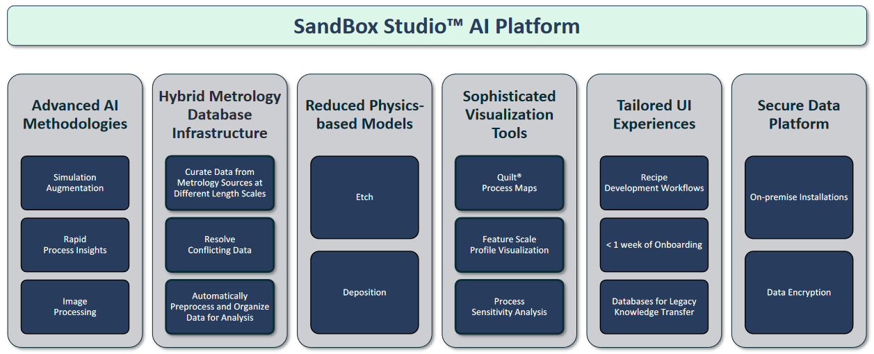 The SandBox Studio AI Platform (Source: SandBox)
I was just about to tell you about the great visualization tools provided by SandBox Studio AI Platform, such as the Quilt process map, but then I found myself in possession of the following image, which pretty much explains itself.
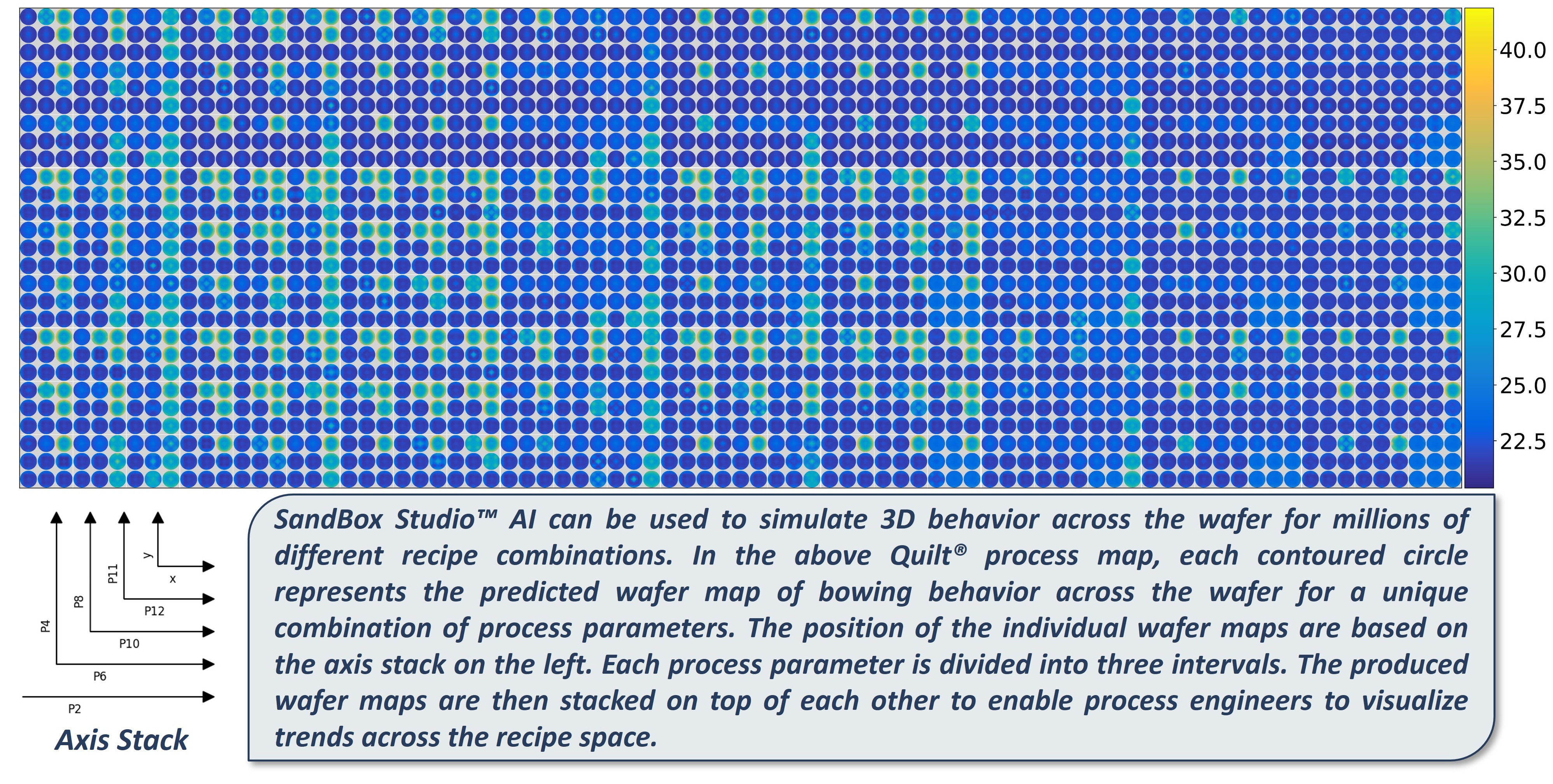
Quilt process map (Source: SandBox)
But wait, there’s more! The reason Meghali wanted to chat with me in the first place was to tell me about a new tool called Weave that they recently added to their toolbox of tricks. To be honest, I couldn’t describe this any better than the following, which I just snaffled from their press release:
SandBox Studio AI’s new product, Weave, significantly improves metrology accuracy and precision by utilizing advanced machine learning capabilities to extract and analyze profiles from SEM and TEM data. Process development engineers can spend up to 20% of their time manually measuring SEM and TEM images. With Weave, process engineers minimize tedious manual tasks and increase metrology accuracy, resulting in more insights, quicker experimentation, and reduced costs during process definition, ramp-up, and high-volume manufacturing.
Weave plugs directly into SandBox Studio AI’s modeling platform providing engineers with an efficient method to curate data from metrology sources at different length scales, resolve conflicting data, and preprocess and organize data for modeling and analysis. This holistic solution reduces metrology costs, improves metrology and model accuracy, and accelerates process development.
Hang on a minute. “Quilt”… “Weave”… Is it just me, or are you also starting to see a pattern here? (“Pattern” – I can’t help myself!) The idea is that once you’ve come up with a new version of your recipe and you’ve used it to do something to your wafer, you then take photos of that wafer (well, cross sections of different devices) and feed them into Weave, which performs tasks like automatic image segmentation, automated material identification, and automatic measurement capture to see if what you got was what you expected and, more importantly, if it’s what you want.
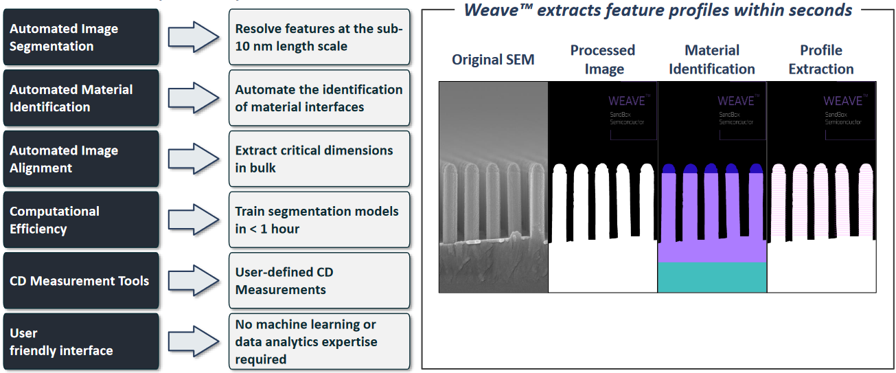
Weave reduces overall metrology costs, increases image processing accuracy, and accelerates process development (Source: SandBox)
What can I say? I’m a sucker for great graphics and I really like the way the following image gathers a bunch of things together in a way that even I can understand what’s going on.
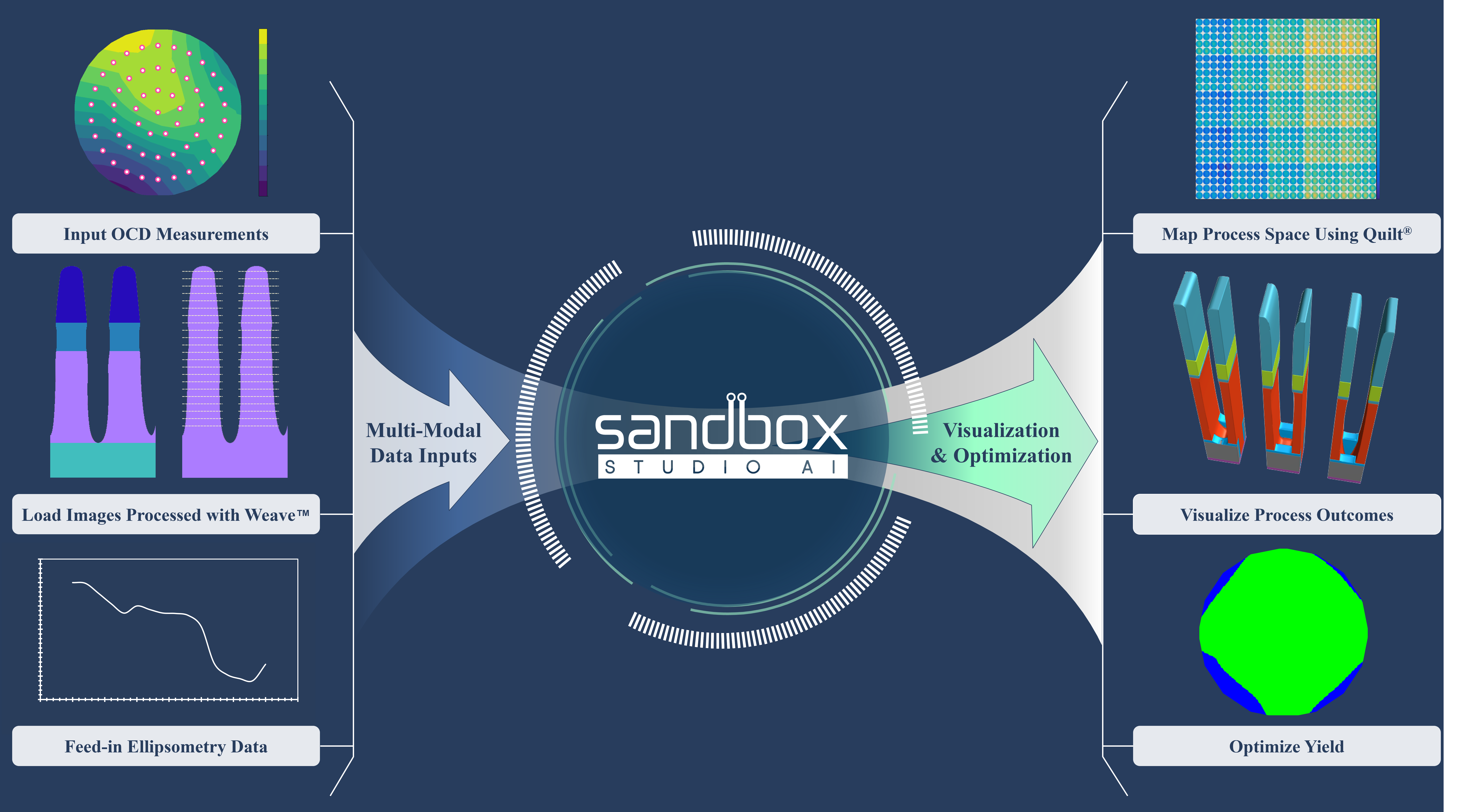
Another look at the SandBox Studio AI Platform (Source: SandBox)
On the off chance you are as excited as me by all this and you can’t wait to tell your family and friends, a quick summary of a few key features of the SandBox platform are as follows:
- SandBox develops AI-based, computational modeling software tools for process engineers to accelerate their semiconductor process development.
- The SandBox Studio AI platform allows process engineers to easily build and deploy custom AI without a single line of code. This enables engineers to realize the benefits of advanced computational models without inhibiting their day-to-day process development.
- SandBox Semiconductor’s AI platform accelerates and reduces the cost of process development for equipment manufacturers and chip manufacturers by 8X.
- SandBox’s new image processing tool Weave automates the extraction of profile information from SEM and TEM images, freeing up engineering time by 20%.
- Weave is a key component of SandBox Studio AI’s hybrid metrology infrastructure. Hybrid metrology is critical to the manufacturing of next generation logic and memory devices.
Hmmm. Perhaps I should have led this article with this summary, but then we wouldn’t have experienced the fun of getting to where we are right now.
The exciting thing for me is that a company like SandBox exists and has been working with foundries and equipment makers for the past several years. The problem they address is very niche, but it’s becoming more critical as the world increasingly relies on advanced chips and manufacturing processes.
Also, as we’ve noted before, the CHIPS and Science Act, which was signed into law by President Biden on 9 August 2022, includes ~$52 billion for American semiconductor research, development, manufacturing, and workforce development. As a result, several companies have unveiled plans for new US-based fabs, and I bet the process engineers in those fabs will be clamoring to use the SandBox Studio AI Platform to help them develop, evolve, and finetune their processes to be the best that they can be.
As always, of course, I will be interested to hear your captivating comments, insightful questions, and sagacious suggestions. So, what do you think about all of this?


One thought on “Accelerating and Reducing the Cost of Semiconductor Process Development”