

Do you remember those dim and distant days when the term AI (artificial intelligence) wasn’t on everybody’s lips? I’m aware that researchers and academics have been beavering away on AI since the Dartmouth Workshop in the summer of 1956, but for decades their labors rarely impinged on the public’s collective consciousness.
Admittedly, the topic of Expert Systems did raise its ugly head circa the 1990s, but these little scamps rarely managed to live up to the marketing hype. Even worse, once those rascally marketeers were exposed to the AI moniker, they began to stamp “AI Inside” labels on anything that moved, even when it was meaningless to do so (in the same way today’s marketing scoundrels sneak “Gluten Free” labels on foods that never had a hint of a sniff of a whiff of gluten to begin with).
By the end of the 1990s, things had gotten so bad that AI—being associated with unfulfilled expectations and broken promises—had acquired a bad name. To be honest, I’d largely forgotten about this technology until it leapt onto the center of the stage with a fanfare of Flubas (which is not something you expect to see on a daily basis) circa the mid-2010s.
Now, just a few short years later, AI is all around us. Earlier today, for example, I was using my Apple Pencil in conjunction with the Nebo app on my iPad Pro. My handwriting is so bad it makes doctors look like they capture their comments in a Copperplate hand. By means of multiple artificial neural networks (ANNs), however, nimble Nebo can understand my handwritten scrawls and convert them into legible text. I stand in awe.
Accompanying the rapid pace of AI development and deployment is the increasing need for computational power and memory. Consider, for example, the current incarnation of the ChatGPT large language model (LLM), GPT-4, which employs a trillion parameters. This is why AI data centers deploy processing beasts like AMD’s MI300X—targeted at tasks like LLM model training and inference for Generative AI (GenAI) workloads—which comes equipped with 192GB of memory and provides 1,800 tera operations per second (TOPS).
Processors and system-on-chip (SoC) devices intended for high-end data center operations of this ilk often make use of High Bandwidth Memory (HBM), which involves stacks of DRAM dice and an optional base die that can include a controller, buffer circuitry, and test logic.
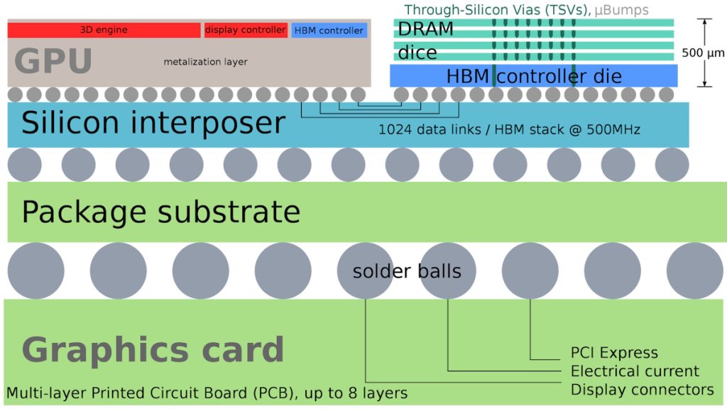
Example device using HBM (Source Wikipedia/Shmuel Csaba Otto Traian)
HBM stacks currently boast 4 or 8 dice, with 12-dice incarnations on the way. These stacks can be presented alongside the processor or accelerator die on a silicon interposer as illustrated above, or they may be mounted directly on the CPU, GPU, or SoC die.
But that’s not what I want to talk about. I’m sorry. I was just setting the scene. At the other end of the spectrum we have Embedded, Edge, and IoT systems, many of which are size- and power-constrained. These systems increasingly involve the combination of sophisticated sensors and AI. I personally like the term Artificial Intelligence of Things (AIoT). According to the IoT Agenda, “The AIoT is the combination of artificial intelligence (AI) technologies with the Internet of Things (IoT) infrastructure to achieve more efficient IoT operations, improve human-machine interactions, and enhance data management and analytics […] the AIoT is transformational and mutually beneficial for both types of technology as AI adds value to IoT through machine learning capabilities and IoT adds value to AI through connectivity, signaling, and data exchange.” I couldn’t have said it better myself.
The reason I’m waffling on about this is that I was just chatting with Chin-Shu “CS” Lin, who is head of Marketing at Winbond. Established in 1987, Winbond is a specialty memory IC company, taking things from research and development, product design, and wafer fabrication, all the way to the marketing of brand name products. Winbond’s major product lines include Mobile and Specialty DRAM (including pseudo-SRAM and HYPERRAM targeted at AIoT applications), Code Storage Flash Memory, and TrustME Secure Flash.
I’ve been writing about chiplets quite a lot recently (see Cheeky Chiplets Meet Super NoCs, Are You Ready for the Chiplet Age? and Chiplets for the Unwashed Masses and Is This the Future of Chiplet-Based Design? and Is This the Ultimate Chiplet Interconnect Technology?), so I was delighted to hear that the guys and gals at Winbond will be providing chiplet-based memory subsystems, as evidenced by the fact that they recently joined the UCIe Consortium.
As part of our conversation, Chin-Shu noted that processing and memory requirements are also increasing in Embedded, Edge, and IoT devices. As one example, we discussed YOLO (You Only Look Once), which is a state-of-the-art real-time object detection system. In 2020, YOLO v4 required ~0.15GB and ~1 TOPS; in 2021, YOLO v5 required ~0.5GB and 3 to 5 TOPS; and, by 2022, YOLO v7 required about ~1.5GB and 5 to 10 TOPS. More recently, in 2023, a new model from Meta AI called SAM (Segment Anything Model) that can “cut out” any object, in any image, with a single click requires ~4GB and >20 TOPS (see a demo here).
Powerful Embedded, Edge, and IoT devices are the markets the chaps and chapesses at Winbond will be playing in with their recently introduced CUBE architecture. CUBE, which stands for Customized Ultra Bandwidth Element, is based on Winbond’s DRAM technology and is part of Winbond’s known good die (KGT 2.0) initiative.
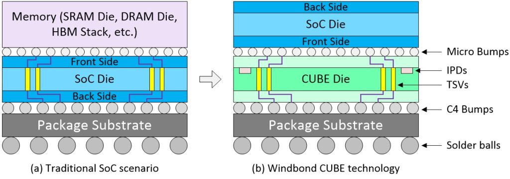
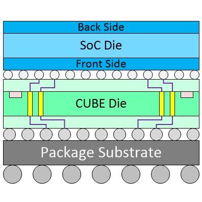
Comparison of traditional vs. Winbond CUBE implementations.
In the image above, we see a brace of scenarios for SoC designers aiming at the smallest package possible. The traditional solution (a) is to flip the memory device over and mount it on the front side of the SoC die. In turn, this requires the SoC die to employ TSVs (through-silicon vias), which consume valuable silicon real-estate. By comparison, in the case of Winbond’s CUBE technology (b), it’s the SoC die that’s flipped and attached to the CUBE die.
This CUBE approach offers multiple benefits, starting with the fact that having the SoC die on the top provides better power dissipation. Also, not having TSVs in the SoC die reduces cost, complexity, and area. Furthermore, the CUBE die can include integrated passive devices (IPDs) like silicon capacitors (Si-Caps), which help provide the SoC with stable power without requiring myriad discrete multilayer ceramic capacitors (MLCCs). The real value-add here is that the CUBE can provide a functionality troika by acting as DRAM + Si-Caps + SI-Interposer.
Each core SRAM cell requires 6 transistors. Each core DRAM cell requires only 1 transistor. As a result, using a relatively cheap 20nm process, the CUBE offers 5X the density as an SRAM die implemented at the relatively expensive 14nm process. Also, the CUBE is extremely power efficient, consuming only ~1 picojoule per bit. The initial CUBE involves only a single die, but multi-dice stacked versions are on Winbond’s roadmap.
As usual, we’ve only scratched the surface of what’s possible here, so please reach out to the folks at Winbond if you want to know more (tell them “Max says Hi”). And, as usual, I welcome your insightful comments, perceptive questions, and sage suggestions.


