

I can’t believe it; we’ve finally arrived at the ultimate part of what started out as a mini-series and ended up being a mega-epic. In a moment, we’re going to consider FPGA (hardware) and MCU (software) solutions to the switch bounce problem, but first…
Just in case you arrived late to the party, in Part 1 we introduced the concept of switch bounce; in Part 2 we delved deeper into the bouncing associated with SPST and SPDT switches; in Part 3, Part 4, and Part 5 we considered how to debounce our switches using RC networks, monostable multivibrators, and latches, respectively; in Part 6 we introduced some special switch debounce integrated circuits (ICs); and in Part 7 we considered switches with resets, switches with interrupts, and polling vs. interrupt-driven techniques. (If any of the terminology above is unfamiliar, you might want to take a look at the associated Switch Types and Switch Terminology columns.)
Fabulous FPGAs
In many systems, any FPGAs are far-removed from any switches, in which case switch bounce is a non-issue for the designer(s) of the FPGA(s). Of course, there’s always “the exception that proves the rule” — that is, a system in which one or more switches are connected directly to an FPGA’s inputs — and that’s what we’ll consider here.
One of the things about today’s FPGAs is that they are so hard to pin down. For example, you could be working with an FPGA that boasts one or more hard processor cores and/or you could configure some of the programmable digital fabric to implement one or more soft processor cores.
If you decide to use one of these embedded processors to perform your switch debouncing, then you can use any of the software solutions discussed later in this column. Alternatively, you could use one or more of the externally implemented hardware debounce solutions we’ve introduced in previous columns. For the sake of our discussions here, however, we will assume that you intend to use the programmable digital fabric inside the FPGA to debounce your switches.
As an aside, irrespective of the solution you opt for (software, external hardware, internal hardware), one of the things you will have to consider is the possibility of metastability that might be triggered when an asynchronous transition on a switch meets the synchronous world inside the FPGA. We are going to ignore this here, because metastability is a topic for another day (or next week, depending on how many comments I see clamoring for a column on this subject).
As fate would have it, I personally have never been obliged to implement a switch debounce solution using the programmable fabric inside an FPGA. Obviously, this lack on my part had the potential to severely curtail this portion of our discussions. Happily, I know people who know stuff (“It’s not what you know, it’s who you know,” as the old saying goes).
For example, my chum Jonny Doin, who designs safety-critical embedded systems for things like nuclear power plants, emailed me to say:
Max, I’m enjoying this series very much. Debounce is one of those things you always will have in any project. In FPGAs, bouncing inputs can wreak havoc in your FSMs and find nasty bugs in your sequential logic. Sometimes you have to group switches that are related (like multi-pole switches) and need to be latched all at the same time. Such is the case in a VHDL Debouncer Circuit I shared a long time ago in OpenCores that is still getting downloaded.”
Also, a man we’ll call Brian (because that’s his name) posted a comment to Part 1 of this mini-series/mega-epic saying:
Max, as you likely recall, there was some great discussion regarding this subject on the late All Programmable Planet website, before it was so ruthlessly destroyed by the Vogon contingent at UBM & Xilinx to make way for an interstellar billboard without bothering to create a read-only public archive! With that whinge (mostly) out of the way, my favorite technique (as I once described so eloquently on the aforementioned website, before those posts were, “lost in time, like tears in rain”) for FPGA switch input debouncing is a minimal hardware circuit of about a half dozen flip-flops per input to debounce. This uses a common time-base counter, shared by all inputs, that performs the debounce function with a glitch-detecting sampler like the logic analyzers of yore used at low sample rates. If one has, say, 50 inputs to debounce, this approach requires much less hardware than does a counter-per-input-pin debouncer. You can download the example VHDL debouncer and testbench.”
And then we have Mike Fitzgerald, who is an FPGA Design Engineer at Motorola Solutions. Mike really went above and beyond the call of duty with this one after we’d chatted on the phone when he sent the following message:
Hi Max, can you log into edaplayround.com and run the code at this link. This is the SystemVerilog debounce and testbench we discussed. There are about 100 lines of RTL and 100 lines of testbench. It’s based on using a counter to count consecutive 0s or 1s in order to make a state change. There are two parameters used to define the number of consecutive 0s or 1s. I’ve set both of these to be 10 in order to view a tractable amount of time. Of course, values of 10 are not realistic in the real world of nanosecond (ns) clocks, but they make the simulation waveforms nice to look at and the simulation runs quickly. The design is parameterized so that any number of clock cycles (number < 2^31 – 1) can be used as the 1->0 and 0->1 thresholds. So, if a user had a 1 ns clock and required a solid 1 millisecond (ms) of 1s to change from 0->1, they would set the appropriate parameter to be 10^6.
Well, I don’t know about you, but my FPGA cup runneth over. However, I think we’ve had enough dilly-dallying and shilly-shallying — it’s finally come time to consider, contemplate, cogitate, and ruminate on a smorgasbord of software solutions with which we can debounce our pesky switches.
Software Solutions (Ground Rules)
Before we leap headfirst into the fray with gusto and abandon, let’s first set some ground rules. Let’s start with the fact that I’m a hardware design engineer by trade and my software leaves something to be desired, so ground rule #1 is that you aren’t allowed to laugh at and/or criticize my code.
Actually, now I come to think about it, I will be using a pseudo-code of my own devising, thereby making it hard for you to tell me I’ve got it wrong (I’m a problem solver at heart).
The next point is that we are initially going to assume we are working with a single switch — we can scale our solution to handle multiple switches later.
Let’s also suppose we have some master clock “tick” — say once every millisecond — and that we use this tick as the impetus to check the state of our switch. One way to do this, as embedded guru Jack Ganssle noted in his classic Guide to Debouncing article, is to “…respond to tick interrupts, say once a millisecond, like you’d normally do with an RTOS or timer, and quickly sample the GPIO switch input. A pretty simple algorithm does the debounce. It might take a half-dozen of those interrupts to completely debounce the switch, but this consumes few CPU cycles. This is nice as there’s no waiting in loops for bouncing to settle.”
In the case of the code I create for my hobby projects, I use a similar concept in that I tend to have a main loop that executes once every tick. Remembering that you aren’t allowed to laugh, the Arduino-inspired pseudo-code for this might look something like the following:
#define TICK 1 // Tick time = 1 ms
#define MAX_BOUNCE 20 // 20 ms
uint32_t PreviousTime;
void setup ()
{
PreviousTime = millis();
}
void loop ()
{
uint32_t currentTime;
currentTime = millis();
if ( (currentTime – PreviousTime) >= TICK)
{
// Do stuff with switches
// Do other stuff
PreviousTime = currentTime;
}
}
The Arduino’s millis() function returns the number of milliseconds since the program started running. With regard to MAX_BOUNCE, depending on how we decide to play things, this could be used to say that we are sure the switch will have stopped bouncing 20 ms after the first switch transition, or it could be used to wait until 20 ms after the final switch transition.
Software Solutions (SPST Quick-and-Dirty)
Let’s assume that we are working with a single pole, single throw (SPST) switch as illustrated below: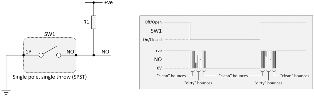
Switch bounce on an SPST-NO toggle switch without noise (Image source: Max Maxfield)
Let’s also assume that the microcontroller pin connected to the switch is called swPin, that we load the value from this pin into a local variable called swValue, and that we keep track of the state of the switch in a global variable called swState.
Bearing all this in mind, a quick-and-dirty solution would be as follows:
// Do stuff with switches
swValue = digitalRead(swPin);
if ( (swState == SW_INACTIVE) && (swValue == SW_ACTIVE) )
{
// Do whatever switch stuff we want to do
swState = SW_ACTIVE;
delay(MAX_BOUNCE * 1000);
}
else if ( (swState == SW_ACTIVE) && (swValue == SW_INACTIVE) )
{
// Do whatever switch stuff we want to do
swState = SW_INACTIVE;
delay(MAX_BOUNCE * 1000);
}
// Do other stuff
I can almost feel professional programmers cringing when they see this, because it’s horrible on so many levels. First, the Ardunio’s delay() function is a blocking function, which means it just sits there twiddling its metaphorical thumbs until the specified delay in milliseconds times out. Meanwhile, it prevents any other actions from taking place.
Quite apart from anything else, our loop will be happily executing once every millisecond until a switch transition occurs, at which point it will lock-up for 20 milliseconds before starting to run again.
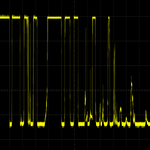
There are ways around this, but — to be honest — they hardly seem worth considering because of the other problems with this solution, not least of which is the fact that it’s susceptible to noise as illustrated below:
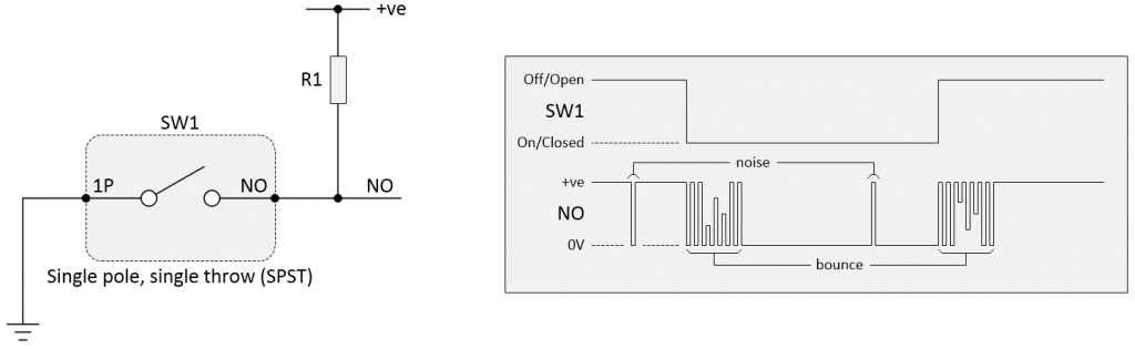
Switch bounce on an SPST-NO toggle switch with noise (Image source: Max Maxfield)
If you look at our pseudo-code above, it’s obvious that if we happen to sample the state of the switch in the middle of a noise spike, then we will mistakenly assume that a real transition has taken place. At this point, things can really go pear-shaped because — in addition to performing any switch-related actions that we really didn’t want to do — our program can easily end up thinking the switch is in the opposite state to the one it actually inhabits.
Software Solutions (SPDT Quick-and-Dirty)
While we are here, this is probably as good a time as any to consider the idea of using a single-pole, double throw (SPDT) switch. If you cast your mind back to Part 5, you will remember that the crème de la crème of hardware debouncing solutions was to use a SPDT switch in conjunction with an SR latch.
In addition to removing the switch bounce, the latch also allowed us to reduce the two switch terminals (NO and NC) to a single signal to be fed to the microcontroller. Well, suppose we remove the latch and feed the NO and NC signals from the SPDT switch directly into the microcontroller as illustrated below:
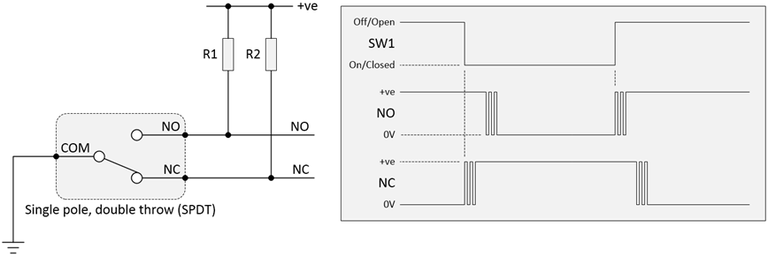
Switch bounce on an SPDT toggle switch without noise (Image source: Max Maxfield)
Obviously, we’re going to need a few more variables to keep track of things, but we can perform a mental experiment. Let’s assume that we start off with the switch in its SW_INACTIVE state as illustrated above, in which case the NO signal is logic 1 and the NC signal is logic 0.
So, we commence by waiting for the NO signal to undergo its first 1-to-0 transition, at which time we perform whatever switch-related actions we wish to perform and set the switch state to SW_ACTIVE. Next, we wait for the NC signal to perform its first 1-to-0 transition, at which time we perform whatever switch-related actions we wish to perform and return the switch state to SW_INACTIVE.
If you have microcontroller pins to spare, then using an SPDT switch with a good software debounce solution is a good way to go. Of course, I haven’t actually presented a good debounce solution yet. Once again, an SPDT variation on the quick-and-dirty SPST concept proposed above could easily run into problems in the case of an occasional noise spike.
Now, the chances of actually sampling a noise spike may be fairly small in the scheme of things, especially when you consider the narrowness of the spikes compared to the relatively vast amounts of time between transitions on the switch (unless you are in a horribly noisy environment, in which case you have all sorts of other problems to worry about), but “fairly small” can quickly translate to “horrendously huge” in the case of a mission-critical or safety-critical application.
What we need to do is to discard our quick-and-dirty (a.k.a. cheap-and-cheerful) solutions and consider something more robust, which we shall do in my next column.
Next Time
I know, I know. I started this column by saying: “I can’t believe it; we’ve finally arrived at the ultimate part of what started out as a mini-series and ended up being a mega-epic…” In a curious example of symmetry, I’m going to end it by saying: “I can’t believe it; against all odds, we haven’t finally arrived at the ultimate part of this mini-series/mega-epic.”
With the benefit of hindsight (the one exact science in which we all have 20/20 vision), we should have described this column as being the penultimate part, but life is a learning experience. What can you do?
On the bright side, all we have left for the most ultimate of ultimate columns is the really, really cool stuff, which will give us all something to which we can look forward. Until that glorious day, as always, I welcome your comments, questions, and suggestions.


This series was exceptional, thank you for doing it. I actually liked the humor too.