

As we discussed in Part 1 of this miniseries, when we operate a switch, it may bounce multiple times before coming to rest in its new state (see also my Switch Types and Switch Terminology columns). This is caused by the fact that the contacts in switches are usually made of springy metals. When they strike together, their momentum and elasticity can cause them to bounce apart one or more times before making steady contact. Depending on who you are talking to, this may be known as “switch bounce,” “contact bounce,” or “chatter.”
The result is a rapidly pulsed electric current instead of a clean transition from zero to full current when the switch is turned On, and vice versa when the switch is turned Off. Switch bounce is not an issue in some applications like power circuits (e.g., a wall-mounted light switch), but it can cause problems in logic circuits and microcontroller-based systems that respond fast enough to misinterpret the OnOff pulses as a stream of data.
Bouncy Bouncy
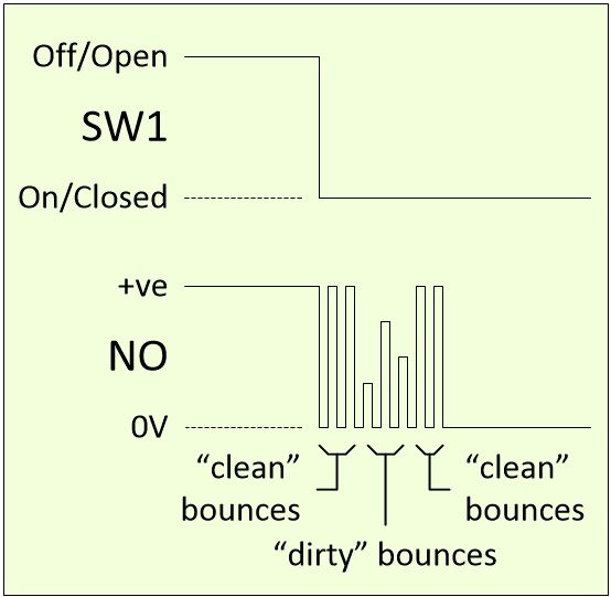
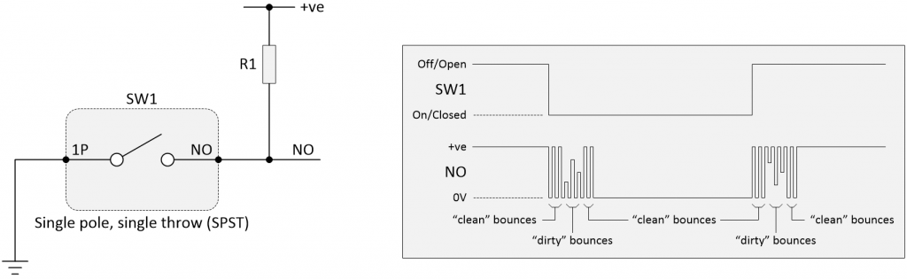
Switch bounce occurs on all the switches we commonly use, such as toggle switches, rocker switches, and pushbutton switches (paradoxically, the only switches that aren’t affected are the ones we rarely use, like mercury tilt switches, for example). It also occurs both when the switch is closed and when it opens again. Let’s start with an SPST-NO (single pole, single throw, normally open) toggle switch as illustrated below.
Switch bounce on an SPST-NO toggle switch (Image source: Max Maxfield)
Sometimes, the bounces go all the way between +ve and 0V. Let’s call these “clean” bounces.
Sometimes the signal doesn’t transition the whole way, but instead oscillates back and forth between the initial value and some intermediate voltage. Although this isn’t official terminology, let’s call these “dirty” bounces. And sometimes we have a random mixture of bounce types.
The only constant is change, because each switch behaves in its own unique way. Even worse, as noted in my previous column, “the same switch may vary its characteristics depending on the temperature, humidity, time of day, direction of the prevailing wind, and the color of your plaid polyester golf trousers.”
Next, let’s consider an SPDT (single pole, double throw) toggle switch as illustrated below (we’ll only show clean bounces for the sake of simplicity).
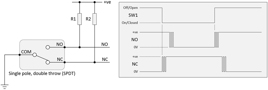
Switch bounce on an SPDT toggle switch (Image source: Max Maxfield)
Note that we are assuming our switch is of the break-before-make (BBM) category, also known as a “non-shorting switch,” which is the most common flavor. As discussed in my Switch Terminology column, this means the moving contact breaks the existing connection with the current throw before making a new connection with the other throw.
In the case of switch bounce, this means that we first see bouncing on whichever terminal is breaking (opening), followed by a short delay, followed by bouncing on whichever terminal is making (closing).
With regard to the circuit shown above, and assuming that logic 0 = 0V and logic 1 = +ve, this means that the NO and NC terminals are 10 and 01 when the switch is in a stable state, and (potentially) 11 in the case of “clean” bounces when it’s transitioning between states, but never 00. Is this significant? Well, it might be if you decide to perform debounce in software on an SPDT switch (which isn’t likely, frankly, because it would use two of your microcontroller’s pins per switch, but we live in an uncertain world, and all things are possible).
Noisy Noisy
In the not-so-distant future, we are going to discuss different techniques for addressing switch bounce. One thing we need to keep in mind is the potential for noise, which may originate from a variety of sources, including crosstalk (from other cables in the system), EMI (electromagnetic interference) from currents in cables, RFI (radio frequency interference) from radio systems that are radiating signals, ESD (electrostatic discharge) from, for example, someone touching the system (see also Adventures in ESD), and natural causes such as electrostatic interference and lightning.
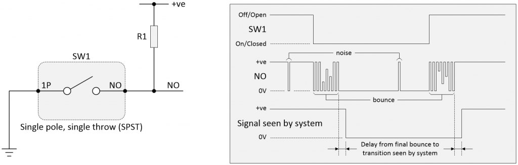
The switch bounce solution must not be fooled by noise (Image source: Max Maxfield)
Unless the designers have accounted for this, reset signals are particularly prone to problems because they tend to meander all over the place. In the case of an Arduino-based system, for example, the reset signal on the motherboard is fanned out to any daughter cards (shields).
As an aside, if you want to learn more about RFI, EMI, and EMC (electromagnetic compatibility), you might want to touch base with Ken Wyatt of Wyatt Technical Services and check out his seminar and presentation offerings, but we digress…
It’s important that whatever technique we use to address switch bounce – pre-processing the signal in hardware or post-processing it in software – that technique is not fooled by the occasional noise “glitch” or “spike.” It would be unfortunate if a “self-destruct” sequence were triggered by someone powering up a vacuum cleaner, for example (on the bright side, at least the end of the world would be accompanied by clean carpets).
Empirical Data
How long does switch bounce persist? How wide are the individual switch bounce pulses? How many pulses might we expect to see? Well, I’m glad you asked. The most reliable data I have comes from two of my chums: Jack Ganssle, who is a legend in the embedded systems spacetime continuum, and David Ashton, who hails from Down Under, and who is a legend in his own lunchtime continuum.
Way back in the mists of time, Jack created his own Guide to Debouncing. When I penned Part 1 of this miniseries, I said things along the lines that “the switch bounce problem is rampant” and “there are now so many solutions scattered around the internet — where most young engineers go to satiate their craving for knowledge — that it makes your head spin. On the bright side, some of these offerings actually work; on the downside, their working may be due to chance rather than design.”
Happily, Jack is of a similar mind. In his guide he says, “Surf the net to sample various approaches to debouncing. Most are pretty lame. Few are based on experimental bounce parameters. A medley of anecdotal tales passed around the newsgroups substitute for empirical evidence.”
So, what Jack did was to take 18 different kinds of switches, build a test rig similar to our circuits above with a 5V supply and a 1kΩ pull-up resistor, and then press each switch 300 times, logging the minimum and maximum amount of bouncing for both the opening and closing of the contacts. After discarding two outliers, the remaining switches exhibited an average of 1,557 usec of bouncing and a maximum of 6,200 usec of bouncing. Jack also notes that the width of the individual bounce pulses varies between less than 1 usec and hundreds of usecs.
This loosely ties in with what David found in two columns he wrote: Switch Bouncing Around and SPDT Switch Debouncing with an SR Latch. In David’s case, he told me that the widths of the individual spikes he observed varied “between a few ns to around 100 usec.”
While we’re here, we should probably note that the width of an ESD pulse can range between a couple of nsec and more that 100 nsec, which means an ESD pulse could easily be mistaken for an individual switch bounce event.
And how many bounces might we expect? Well, according to The Art of Electronics by Horowitz & Hill (Page 506 of the Second Edition), “When the switch is closed, the two contacts actually separate and reconnect, typically 10 to 100 times over a period of about 1 msec.” This just goes to show you how undefined this field is, because this book is regarded as the “Electronics Bible” by many engineers, but their value of 1 msec (which is the one I was told as a young engineer) is less than Jack’s average findings, let alone his maximum findings.
One last thing we have to watch out for when it comes to addressing switch bounce is the overall profile of the pulses. I think the way most of us expect to see these would fall in line with the following screenshot from David’s second column.
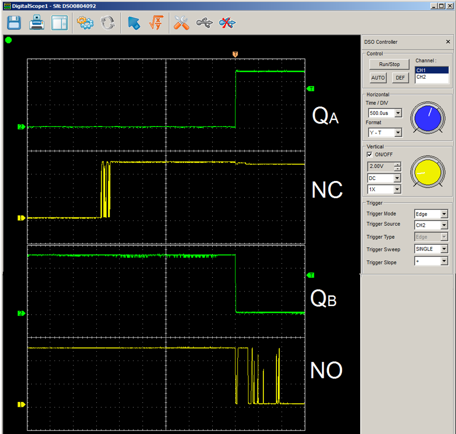
Waveforms for an SPDT switch feeding an SR latch (Image source: David Ashton).
In this example we are turning an SPDT switch Off, so the first thing we see is the NC terminal transitioning from 0 to 1 with some bouncing as it breaks (opens). After a delay, the NO terminal commences its transition from 1 to 0 with some bouncing as it makes (closes). It’s the initial falling edge on the NO terminal that causes the SR latch to toggle, as reflected by its QA and QB outputs.
The point of all this is that the switch bouncing is gathered close to the initial transitions on the NC and NO terminals, which doesn’t seem all that surprising. But things aren’t always this neat and tidy. In Jack’s paper, for example, he notes the following about his O and Q switches (the diagrams below are just my cheap-and-cheerful interpretations – you can see the originals in Jack’s paper).
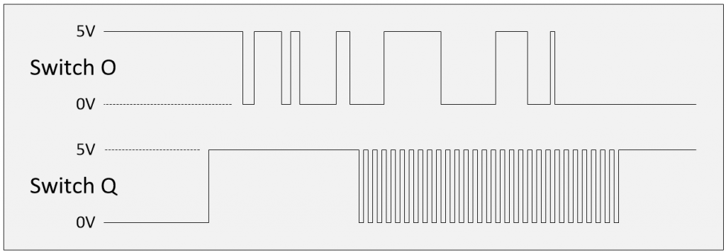
Bounce patterns seen for Jack’s switches O and Q (Image source: Max Maxfield from Jack’s original)
As Jack says in his paper: “O is a very nice, high quality microswitch which never showed more than 1.18 msec of bouncing. But digging deeper I found it usually generated a pulse train guaranteed to play havoc with simple filter code. There’s no high-speed hash, just hard-to-eliminate solid ones and zeroes. One actuation yielded 7 clean zeroes levels ranging in time from 12 to 86 µsec, and 7 logic ones varying from 6 to 95 µsec. Easy to filter? Sure. But not by code that just looks for a couple of identical reads.”
In the case of switch Q, Jack says: “Q, when released, goes high for 480 usec before generating 840 usec of hash – a sure way to drive an interrupt system mad if poorly designed.”
Next Time…
Well, I think we’ve adequately set the scene; now we’re ready to rock and roll. In my next column, we’ll delve into the various hardware and software techniques we can use to convert our naughty bouncing signals into crisp, clean equivalents our mothers would be proud of.


