

In Part 1 of this miniseries, we introduced the concept of switch bounce; that is, when we open (deactivate) or close (activate) a switch, it may make multiple transitions before eventually settling in its new state (see also my Switch Types and Switch Terminology columns). We also noted that this occurs in toggle switches, rocker switches, pushbutton switches, and so-forth — pretty much everything apart from the switches most of us never use anyway, like mercury tilt switches, for example.
In Part 2, we took a deeper dive into the bouncing associated with single pole, single throw (SPST) and single pole, double throw (SPDT) toggle switches, including some empirical data as to how long switch bounce might persist, how wide the individual bounce pulses might be, and how many bounces we might expect to see. Also, we introduced the point that whatever technique we use to address switch bounce – pre-processing the signal in hardware or post-processing it in software – it’s important that the technique is not fooled by the occasional noise “glitch” or “spike” caused by crosstalk, EMI, (electromagnetic interference), RFI (radio frequency interference), or ESD (electrostatic discharge).
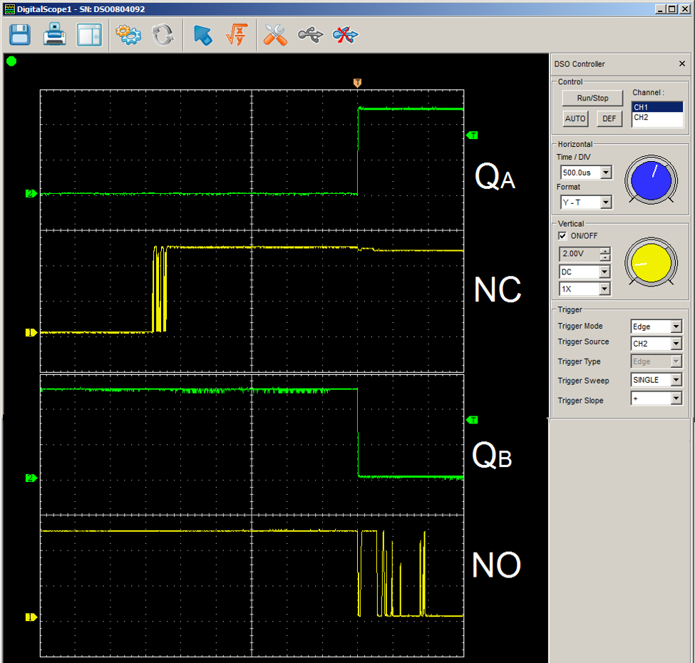
The switch bounce solution must not be fooled by noise (Image source: Max Maxfield)
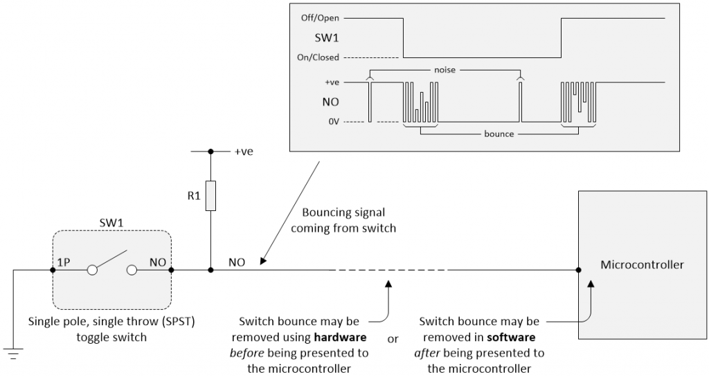
In this diagram, resistor R1 is acting as a pull-up resistor. When the switch is open, R1 pulls the NO signal up to a +ve (logic 1) value. When the switch is closed, it shorts the NO signal to 0V (logic 0).
Now, in Part 3, we have arrived at the point where the “rubber meets the road,” metaphorically speaking. This is where we start to consider various solutions to our bouncing switches.
Hardware vs. Software (A Bit of History)
When microprocessors first came on the scene circa the early- and mid-1970s, there were relatively large numbers of electronics hardware design engineers around, but relatively few software developers, and most of the guys and gals who did know software worked on the “big iron” mainframe computers or on minicomputers.
Microprocessors at that time were limited in terms of memory and clock cycles (i.e., they had relatively low clock frequencies, so every clock cycle was treasured). A lot of programming was painstakingly performed using assembly language, and — just to increase the fun and frivolity — a lot of the code was created by the hardware design engineers who typically were not conversant with programming in general and with good programming practices in particular.
All of the above goes to explain why many of the early solutions to the switch bounce problem were hardware-based — but wait, there’s more…
The 74xx series of transistor-transistor logic (TTL) integrated circuits from Texas Instruments (TI) first appeared in the scene in the mid-1960s. By the 1970s, printed circuit boards (PCBs) populated by these devices — and similar families from other vendors — were ubiquitous.
Each 74xx device typically contained a handful of jellybean logic gates or functions. For example, the 7400 contained four 2-input NAND gates; the 7474 contained two positive-edge triggered D-type flip-flops, each with its own asynchronous preset and clear; and the 74118 contained six SR latches.
The point is that a PCB could contain hundreds of these 74xx devices and, almost invariably, there were functions left unused — a NAND gate here, an SR latch there, perhaps even a D-type flip-flop that was unaccounted for.
Hardware design engineers saw these uncommitted logic functions as being “fair game” for use in debouncing their switches. One slight “fly in the soup,” as it were, is that it wasn’t uncommon to end up with each switch being debounced using a different technique depending on who was doing the designing and which left-over logic gates and functions were available.
Over time, the digital logic was increasingly consolidated into fewer and fewer devices, thereby reducing the amount of simple “glue logic” functions that were going spare. Also, microprocessor memory sizes grew larger, clock frequencies increased, and more and more people started to develop software.
For all of these reasons, it became increasingly common to address switch debounce in the software. The only teensy-weensy problem here is that the majority of software developers were totally unaware that switches bounced — at least, they were until their systems didn’t work when required, worked when not required, or worked intermittently, at which point they asked the hardware engineers what was going on and started a steep learning curve.
Some of the solutions created by software developers are ludicrously simplistic, while others are eye-wateringly convoluted and complex (which doesn’t mean they work as well as one might hope), but we’ll get to them in a while. First, let’s cogitate and ruminate over the hardware side of things…
Traditional Hardware Debounce: RC Networks
The simplest hardware debounce solution is based on the use of a resistor-capacitor (RC) network. The RC time constant of the RC network, also called tau (τ), is measured in seconds and is equal to the product of the resistance (in ohms) and the capacitance (in farads).
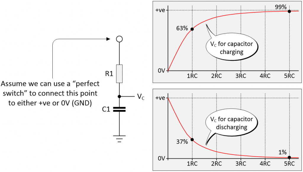
Charging and discharging an RC network (Image source: Max Maxfield)
When a DC voltage is applied to the RC network, then after 1RC the capacitor will have charged to approximately 63% of its final value, and after 5RC the capacitor will have charged to approximately 99% of its final value. Similarly, when the capacitor is being discharged, then after 1RC it will have reached approximately 37% of its final value, and after 5RC it will have reached approximately 1% of its final value.
We can use a variation of this circuit to smooth out the switch bounces as shown below. When we close the switch, it’s like we replaced it with a piece of conducting wire, and the capacitor discharges through resistor R2, so the RC time constant is (R2 * C1). When we open the switch, it’s like we removed it from the circuit, and the capacitor charges through resistors R1 and R2, so the RC time constant is ((R1 + R2) * C1).
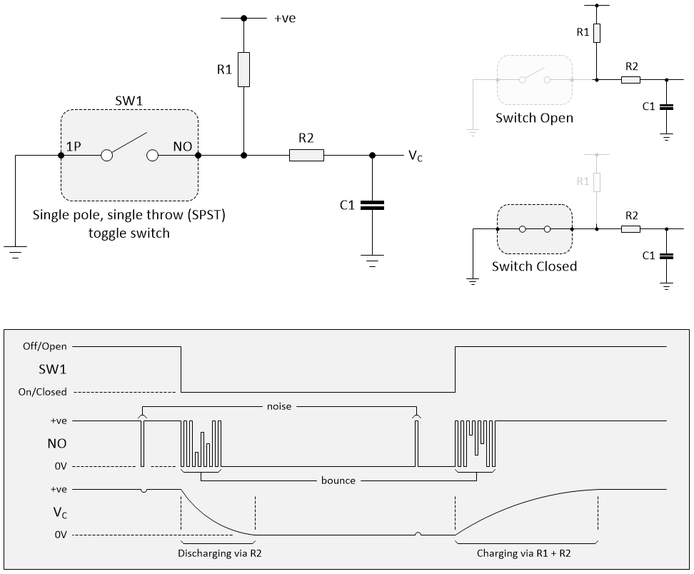
Using an RC network to debounce a toggle switch (Image source: Max Maxfield)
Observe that, if the resistor and capacitor values are selected correctly, any noise spikes will be smoothed out into insignificant blips. The switch bounce will superimpose a ripple on the VC value, but — again — this will be smoothed out if the resistor and capacitor values are selected correctly.
What’s the best way to select these values? Well, in this case I’m going to take the weasel way out and defer to the “Doing the Math” portion of Jack Ganssle’s Paper (may I remind you of the old saying that “Eagles may soar, but weasels rarely get sucked into jet engines”).
One of the problems with the solution shown above is that the charging time when the switch is opened (deactivated) is longer than the discharging time when the switch is closed (activated). This may not be a problem for many applications in which the switch’s activation is considered to be the important part of the process, but if it is required to shorten the deactivation time, then this can be achieved by adding a diode as illustrated below.
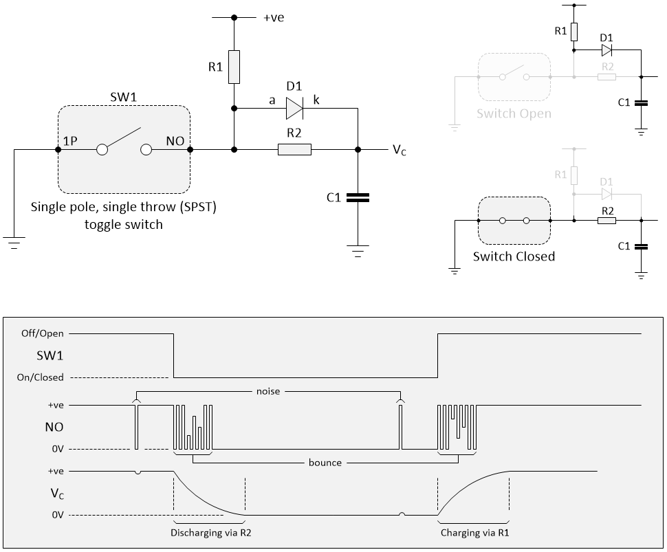
Adding a diode to the RC network (Image source: Max Maxfield)
Purely for the sake of discussion, let’s assume our +ve value is 5V. Let’s also assume that we are starting off with our switch open and the capacitor charged to 5V. This means that when we close the switch, the diode’s cathode (k) is at 5V, while its anode (a) is at 0V. This means the diode is reverse biased, which means it won’t conduct, which means it’s like not having it there in the first place. Once again, the capacitor discharges through resistor R2.
By comparison, when we eventually open the switch again (after the capacitor has been discharged), then the diode’s cathode will be at the capacitor’s 0V and the diode will be forward biased from the 5V supply coming through R1. So long as the difference in potential stays above the diode’s forward voltage drop, the diode will conduct and will appear to be a short circuit, as if it were replaced by a piece of wire. Since we have effectively shorted out R2, it’s as if this resistor were removed from the circuit, so the capacitor charges only through resistor R1.
In the case of a small silicon diode operating at its rated currents, its forward voltage drop is about 0.6 to 0.7 volts (the value is different for other diode types; Schottky diodes can be rated as low as 0.2 V, while germanium diodes are in the 0.25 to 0.3 V range). Thus, assuming a small silicon diode with a forward voltage drop of 0.7 V, the only time R2 will come into play will be when the capacitor is close to the end of its charging cycle when its voltage reaches 4.3 V, which is long after the point when we will have registered the switch as having opened.
We still have one final point to ponder with regard to our RC debouncing solution — the fact that the VC signal has slow rise and fall times. Digital functions prefer to see the signals presented to their inputs as being below a certain value considered to be a logic 0, or above a certain value considered to be a logic 1. These values vary depending on the technology (e.g., TTL vs. CMOS) and the supply voltage (e.g. 5.0 V vs. 3.3 V). In the case of standard TTL with a 5 V supply, any signal below 0.8 V will be considered to be a logic 0, while any signal above 2.0 V will be considered to be a logic 1.
When it comes to a microcontroller-based system, these values also vary depending on the microcontroller (MCU) in question. In the case of the Atmel (now Microchip Technology) ATMega328 MCU, which is used in the Arduino Uno, for example, any value presented to a digital input that’s below 1.5 V or above 3.0 V will be considered to be a logic 0 or logic 1, respectively.
The point of all this is that digital functions in general, and microcontrollers in particular, don’t like to see input signals wandering around in the undefined region between a “good” logic 0 and a “good” logic 1. This is unfortunate, because the gradual rise or fall of the signal coming out of the RC network spends a lot of time (relatively speaking) in this “forbidden zone.”
Fortunately, way back in 1934, a young graduate student called Otto Herbert Schmitt invented something we now know as a Schmitt trigger (this invention was a result of Otto’s study into the propagation of neural impulses in the nerves of squids). The best way to describe this is by means of a figure as illustrated below.
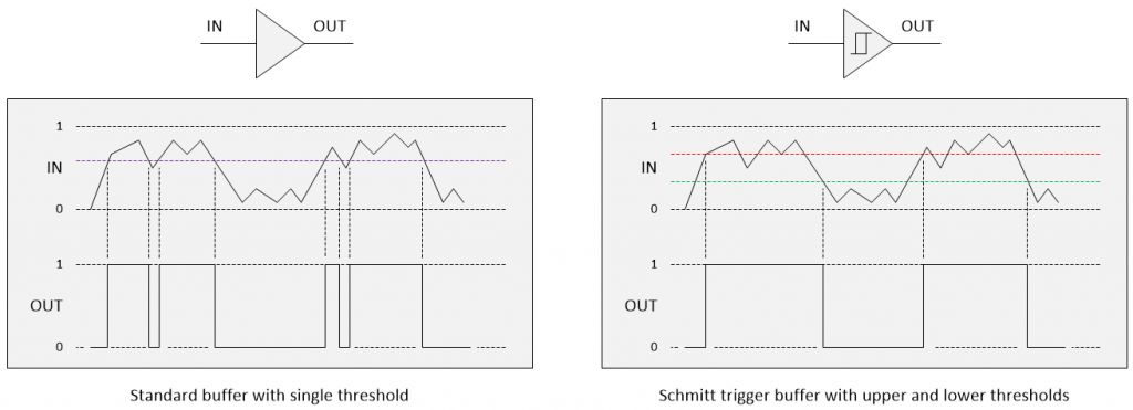
Standard buffer vs. Schmitt trigger buffer (Image source: Max Maxfield)
A standard buffer has only a single switching threshold, which means that a noisy signal — including a signal with a bit of ripple on it — can result in multiple transitions at the output. By comparison, a Schmitt trigger buffer — that is, a buffer with a Schmitt trigger input — has two thresholds. The output changes only when the input crosses the upper threshold or the lower threshold. This dual threshold action is called hysteresis (the dependence of the state of a system on its history), which implies that the trigger possesses memory.
In the case of the RC network that we’re using as a simple SPST switch debounce circuit, we would add a Schmitt trigger buffer between the RC network and the microcontroller as illustrated below.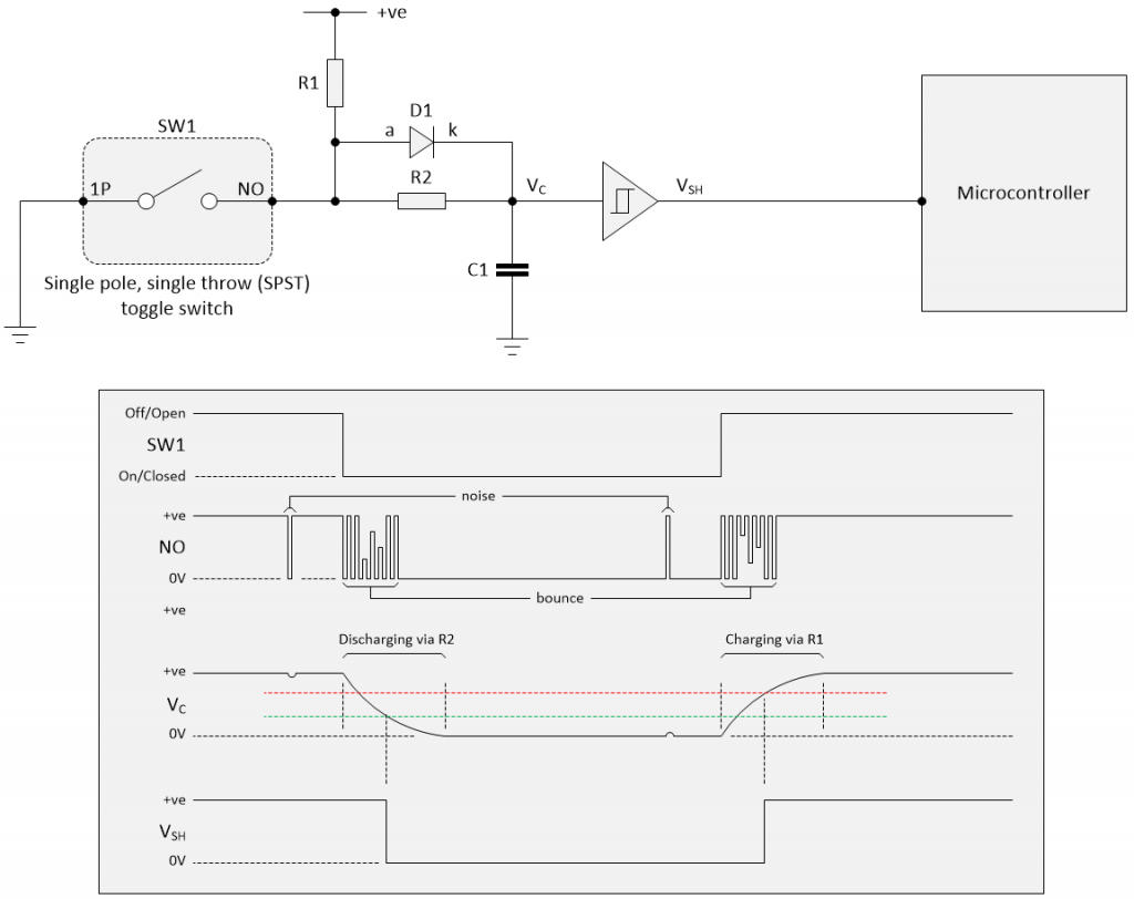
Adding a Schmitt trigger buffer to the RC network (Image source: Max Maxfield)
As one last point, we should perhaps note that the reason we’ve shown a non-inverting Schmitt trigger buffer is to keep things simple (i.e., all of the signals going up and down in the same general direction). In reality, it would be more common to use an inverting Schmitt trigger buffer, because inverting functions are faster than their non-inverting counterparts.
If we did use an inverting buffer, then we’d have to “swap things over” in the software. That is, instead of regarding a logic 0 as representing the switch closing, we would now regard a logic 1 as indicating this switch state, and vice versa.
Call Me Pedantic If You Will
I fear I’ve gone a little overboard with my description of the RC debounce circuit, not the least that we have so many other hardware debounce techniques available to us. However, the purpose of these columns is to answer everyone’s niggling questions. As part of this, I want to explain the hardware side of things in such a way that software folks can understand what’s going on, and — when we eventually get to any software solutions, explain those in such a way that folks on the hardware side of the fence can understand what we’re waffling on about.
I also remember what it was like when I was starting out. People would throw things into the conversation (or written descriptions) without explanation, scattering terms like “reverse bias” and “forward voltage drop” and “Schmitt trigger” like confetti, assuming that I had a clue what they were talking about. Sad to relate, this was often an unwarranted assumption.
What do you think? Do you like the way I’m covering things, or would you like me to pick up the pace?


Im in no position to advise a world famous author on pace, however I have enjoyed this article series and look forward to the next one!
Hi Ted — thanks for your kind words — to be honest it’s only my mom who considers me to be a “world famous author” LOL The funny thing about the topic of switch bounce is that I thought I was pretty conversant with it until I started writing about it — that’s when you begin to examine all the things you were told or read and you start to spot the flaws in many of the purported solutions — I have some amazing stuff to reveal in Part 4 … watch this space …
Hi Max
When I was studying FPGA design in University My lecturer told me to create pushbutton debounce design.
First , I thought that this would be trivial problem and I could finish very fast but then I found out that this is serious problem that needs to be address in every design that uses pushbutton (or any button/switch).
As you already stated I too used web to find example solution and ended up using following design (Link Below) and it worked.
https://www.digikey.com/eewiki/pages/viewpage.action?pageId=4980758
I was using Intel(Altera) Cyclon V GX starter kit.
Thank you for creating this guide 🙂
Hi Pavle — thank you so much for your kind words and also for pointing me at this solution on the Digi-Key website. As you say, what you start off thinking with be a trivial problem quickly becomes… let’s say “interesting” — I’m currently working on the next article in this odyssey — it will be posted tomorrow — I think it may surprise a lot of people — I very much look forward to hearing what you think about it — Max
Thank you for reply Max. I am looking forward to next article.
Great article, Max, and a great series of articles on switch debounce!
You “outsource” the cap charging calcs to this page:
http://www.ganssle.com/debouncing-pt2.htm
Just wanted to draw your attention to this fact:
That page has a schematic of the same “final” RC circuit with the diode – such that charging and discharging can be symmetrical and through one resistor each way. However, as far as I can tell the RC calcs are actually for the circuit without the diode. ie he uses R1 + R2 for charging.
It might be worthwhile pulling out those calcs and making them directly relevant to your text. In fact, when using the diode, the calcs simplify somewhat – the time constant is the same each way, although the thresholds are still different and will depend on your downstream device, probably a Schmitt trigger gate.
The forward voltage of the diode – not mentioned at all on the ganssle.com page , because, despite showing it, he doesn’t discuss this circuit – needs to be dealt with too, ie effectively subtracted from Vcc during the charging time.
It probably needs an example suing the thresholds from an actual downstream device. For example, I am using one of these:
https://www.ti.com/lit/ds/symlink/sn74hc14.pdf
As a second point, it might be worth noting that the preferred Schmitt Trigger devices are most commonly available in an inverting config (like the above device). Inverting types are cheaper, faster and available in more package types. eg there are no non-inverting options in DIP available, for prototyping, at all that I could find. Now this may suit the application, ie you want your reset line to go high when you push the button – it’s a pull down, but that gets inverted – but it may not. So really your article would benefit from showing the “mirror image circuit” which could be used for inverse logic or for use with an inverting, downstream Schmitt trigger device as appropriate.
Many thanks again. Keep up the good work.
Hi Oschonrock — thanks so much for your feedback , now I feel bad because I was being lazy pointing the reader to Jack’s calculations. Regarding bringing the calculations “in house” into this column (and possibly the next one), I will add it to my list of things to do, but I am 100% swamped at the moment.
Re my showing the non-inverting Schmitt trigger device in this column — I don;t disagree with you, but I was trying to take things step-by-step and I didn’t want to introduce two many concepts at once — I swapped over to an inverting device in Part 4 ( https://www.eejournal.com/article/ultimate-guide-to-switch-debounce-part-4/ ).
Once again, thanks for taking the time to provide this feedback — its wonderful to hear from someone who has actually read something I’ve written LOL
This is a brilliantly helpful post, especially with the insistence on looking at /actual/, experimentally-derived data, and the practical impacts of various solutions. Thanks for this.
Dear Max thanks for the amazing post,
I wonder to know, am I correctly calculate the equation based on these assumptions for the schematic with the diode?
Vcc = 3.3
VIL = 0.9
VIH = 1.9
C1 = 100nF
D1 = 0.2 voltage drop
Debounce elimination time = 20ms
When the switch is closed we have :
Vc = VCC (e^(-t/(R2*C1))) -> 1.9 = 3.3(e^(-0.02/ (R2*100nF)
So the R2 is 362K
And when the switch is opened :
Vc = (VCC – Vdiode)(1- e^(-t/(R1*C1)))
So the R1 would be 583K
Are the calculated value for the resistor too high ???
What a great series this is!
I do have a question which I don’t think has been covered here. The RC + Schmitt Trigger circuit works nice, however, during power switch on the capacitor still needs to load (“zero volt” => results in “1” at inverting schmitt trigger output). Once the capacitor is loaded, the output switches back to zero.
Is there a way to avoid this switch on behaviour and keep the output stable during switch on?
Hi there — thanks for your question. Before I answer, I should note that you refer to an inverting Schmitt trigger in your query — I’m actually showing a non-inverting gate in my diagram (I was trying to keep things simple). But I take your point that in the real world most of these devices ARE inverting (a 7413 is a dual 4-input NAND with Schmitt inputs and a 7414 is a hex inverter with Schmitt trigger inputs).
Now, with respect to your question, which basically says that the way my circuit is drawn (with a normally-open (NO) switch), then on power-up, the capacitor will start off at 0V and then charge up, which will probably result in a glitch at the output of the Schmitt buffer or inverter.
There are multiple ways to stop this (or at least prevent it from having an effect):
1) Replace the NO switch with a normally-closed (NC) version. That way the capacitor starts off at 0V and is held at 0V, which means the output from the buffer/inverter won’t glitch.
2) The microprocessor should already be equipped with a hardware power-on-reset (POR) circuit that makes it pause while the rest of the system settles down.
3) Just to be safe, the first line of code in your program could be something like a delay(100) (“do nothing for 100 milliseconds”), which should give the rest of the system (including the system clock) time to settle down.
4) Use an LS18 (3-channel debounce IC) from LogiSwitch (FYI I’m the CTO of LogiSwitch) as described in Part 6 of this series https://www.eejournal.com/article/ultimate-guide-to-switch-debounce-part-6/
Note that of you go to Part 9 https://www.eejournal.com/article/ultimate-guide-to-switch-debounce-part-9/ then you’ll find links to all of the earlier parts.