

Like a battered and bruised prizefighter, phase-change memory (PCM) refuses to stay down or give up the fight. Although it got a black eye and bloody nose from its Micron 3D XPoint and Intel Optane misadventures, PCM has found its way into microcontrollers, thanks to a collaboration between STMicroelectronics (ST) and Samsung. Back in 2018, ST announced that it was sampling microcontrollers with embedded PCM (ePCM) made with a 28nm FD-SOI (fully depleted silicon on insulator) process for the automotive market. Now, ST has announced the next generation of automotive microcontrollers with ePCM, fabricated by Samsung using a jointly developed 18nm FD-SOI process combined with ST’s ePCM technology. ST plans to sample this new 18nm microcontroller to automotive customers in the second half of 2024, with device production planned for the second half of 2025.
It’s extremely pertinent that ST has targeted microcontrollers with ePCM specifically at the automotive industry, which has more severe environmental temperature requirements than most other microcontroller applications. High operating temperatures are PCM’s Achilles heel because of the physical phenomena it’s based upon. PCM exploits the resistance change in a material as it transitions between amorphous and polycrystalline states. The amorphous state has a high resistance, and the polycrystalline state has a lower resistance. The two states create a memory cell. A sharp, short temperature spike from a co-located heater causes the PCM storage medium to assume an amorphous state, while a longer, lower heat pulse causes the material to transition to the polycrystalline state, as shown in the figure below.
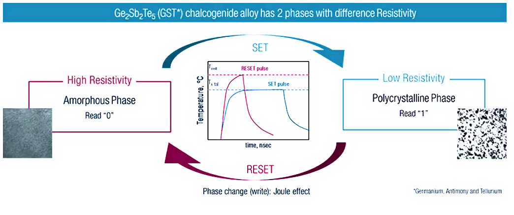
PCM changes from its amorphous state to its polycrystalline state and back through the application of tailored heat pulses. Image credit: ST
High ambient temperatures can anneal the bits right out of a PCM. However, ST rates the maximum operating temperature of its PCM material – made from an alloy of germanium, antimony, and tellurium (GST) – at 165°C, at least for the company’s 18nm automotive microcontrollers, according to the company’s PCM Web page.
The figure below illustrates the PCM cell design. The heaters that drive the phase changes for these PCM cells are buried bipolar transistors.
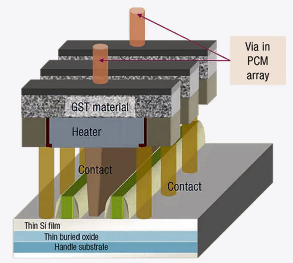
ST’s PCM cell consists of a block of germanium-antimony-tellurium (GST) alloy coupled to a heating element made from a bipolar transistor. Image credit: ST
Basing a new microcontroller family on a memory technology with a long and somewhat sketchy history may seem risky, but there’s a method to ST’s madness. Ever since the 1970s when microcontrollers first appeared, they’ve been largely based on some sort of erasable PROM (EPROM) cell, except for hard ROM versions. The earliest microcontrollers used ultraviolet-erasable EPROM (UV-EPROM) cells. IC vendors packaged these first erasable microcontrollers in packages with quartz windows to permit erasure and reuse. To reduce the price of their devices, they would omit the package window, creating one-time-programmable devices with the same microcontroller die. Later, when the semiconductor industry mastered electrically erasable EPROMs (EEPROMs) and then Flash EEPROMs, packages with quartz windows disappeared entirely.
However, Flash EEPROM cells don’t scale well as the industry rides down the Moore’s Law curve, which pushed ST to find an alternative nonvolatile memory technology that was suitable for use in microcontrollers fabricated using more advanced semiconductor processing nodes. Some microcontroller manufacturers have turned to ferroelectric RAM (FeRAM) or embedded magnetic RAM (eMRAM) for their microcontrollers. ST chose ePCM. (For a review of all these embedded nonvolatile memory technologies, see “Can Any Emerging Memory Technology Topple DRAM and NAND Flash?” and Max Maxfield’s recent article, “Is It Time for MRAM to Shine?”)
ST is no newcomer to PCM. ST formed a new nonvolatile semiconductor memory company named Numonyx in 2008 with Intel as a joint venture partner. Numonyx memory chips used either Flash EEPROM or PCM memory cells. The new company made several types of nonvolatile memories but specialized in NOR Flash memory. Numonyx introduced 90nm PCM devices in 2010. That same year, Micron purchased Numonyx for $1.27 billion worth of stock and got into the PCM game. Micron soon discontinued the Numonyx PCM devices and later introduced a different line of PCM memory chips that it jointly developed with Intel. The company named these new PCM devices “3D XPoint.” Intel introduced its own version of 3D XPoint PCM called Optane, which the company packaged and sold as memory DIMMs and SSDs.
Intel’s Optane and Micron’s 3D XPoint were positioned as direct competitors to NAND Flash EEPROM, but the economics of PCM and the rapid development of NAND Flash devices never allowed 3D XPoint and Optane products to become cost competitive for large nonvolatile memories. Micron exited the PCM arena in 2021, and Intel killed Optane PCM in 2022. (See “Optane, We Hardly Knew Yeh.”) Meanwhile, ST continued to research PCM technology for embedded applications requiring smaller memory capacities.
ST is also no stranger to FD-SOI. The company opened its 28nm FD-SOI process for pre-production orders at the end of 2012. Around that same time, ST and GlobalFoundries (GF) announced that GF would be manufacturing ICs based on ST’s 28nm and 20nm FD-SOI process technology. Samsung licensed ST’s FD-SOI process technology in 2015, and, in 2022, ST and GF announced that they would create a new, jointly operated, FD-SOI-capable 300mm semiconductor manufacturing facility adjacent to ST’s existing 300mm semiconductor fab in Crolles, France. (See “STMicroelectronics and GlobalFoundries Jointly Press on with FD-SOI in a New Fab Near Grenoble.”) This short history brings us to ST’s most recent announcement of its 18nm FD-SOI microcontrollers for automotive applications. Samsung is the initial foundry for the devices, but the jointly held ST/GF fab in Crolles will be available as an alternative manufacturing source. These days, with automotive customers recently traumatized by collapses in the semiconductor supply chain, an alternative supply source looks mighty appealing.
ST has been cagey about the specifications for its new 18nm automotive microcontrollers. The press release simply says:
“The first microcontroller based on this technology will integrate the most advanced ARM Cortex-M core, providing enhanced performance for machine learning and digital signal processing applications. It will offer fast and flexible external memory interfaces, advanced graphic capabilities and will integrate numerous analog and digital peripherals. It will also have the advanced, certified security features already introduced on ST’s latest MCUs.”
When pressed to name the processor core, a spokesperson for ST provided an indirect answer by saying that Arm’s current state-of-the-art Cortex-M processor core was the Cortex-M85. This Arm processor core incorporates Arm’s Helium vector-processing extensions, which can accelerate graphics, DSP, and machine-learning algorithms. Helium is a lighter-weight approach to vector processing compared to Arm’s Neon SIMD vector extensions. Helium is a lighter noble gas than neon, hence the name for this extension to the Arm Cortex-M architecture. The Cortex-M85 processor core also has enhanced security features, which is likely to be appreciated by automotive designers who are fighting a constant battle against bad actors that are trying to develop ever-better ways to hijack or steal vehicles. (See “Meet the CAN Invader – How Can Automotive Ethernet Curb Car Theft?”)
How fast will Arm’s “state-of-the-art Cortex-M” processor in ST’s new 18nm microcontroller run? Again, ST doesn’t say, but microcontroller vendor and competitor Renesas recently introduced a microcontroller family based on a Cortex-M85 processor core, the RA8D1, which clocks at 480MHz. Renesas manufactures its RA microcontrollers using a 22nm process technology, so, potentially, the Cortex-M85 core in ST’s 18nm FD-SOI microcontroller could run even faster than that.
Similarly, ST’s press release makes no mention of the amount of PCM or RAM incorporated into the new automotive microcontrollers. For clues, we can look at ST’s prior generation of automotive microcontrollers based on FD-SOI and PCM. These devices are in ST’s 28nm Stellar microcontroller family. The largest member of this family is the Stellar SR6 P6, which incorporates six Arm Cortex-R52+ processor cores, as much as 2.3 Mbytes of SRAM, and as much as 16Mbytes of PCM, with 15.5 Mbytes of PCM dedicated to storing code and data and 0.5 Mbytes of the PCM dedicated to the microcontroller’s hardware security module. The Stellar SR6 P6 microcontroller also has 15.5 Mbytes of shadow PCM to accommodate over-the-air (OTA) updates.
In jumping from a 28nm to an 18nm FD-SOI process technology, I’d expect that ST should easily be able to double or possibly quadruple the amount of available RAM and PCM on its new microcontrollers. If my guess is wrong, I’m sure ST will let us know, by and by. Eventually, ST will produce data sheets for these new 18nm FD-SOI microcontrollers with additional information. For now, we have the promise of a new and interesting application for the industry’s next-generation FD-SOI process – to be made by Samsung, ST, and GF – and PCM gets to go another round in the semiconductor memory prize fight.


