

I hail from a time when we could do naught but dream of computer memories with the capacity and performance of today’s offerings. On the bright side, I didn’t have to fight my way through using technologies like mercury delay lines. On the other hand, it wasn’t uncommon for the mainframe computers with which I came into contact to have a magnetic core store for main memory coupled with magnetic tape for long term storage.
I remember my first job after graduating university. I was a member of a team designing central processing units (CPUs) for mainframe computers at International Computers Limited (ICL) in West Gorton, Manchester, UK. When I wanted to access a file that I was working on a few hours or days before, I’d enter the appropriate request into the command line interface (CLI). The response was typically along the lines of, “Wait for a while… take a chill pill… we’ll get back to you when we feel like it.”
Eventually I discovered what was going on behind the scenes (“Pay no attention to that man behind the curtain”). My request would appear on an operator’s console in the main computer room. My username and the file name I’d given would be used to determine on which magnetic tape my file had been stored. Then a junior operator would be dispatched to retrieve that tape from the storeroom and load it on the first tape deck to become free. Fortunately, the pace of life was slower back then. I can only imagine what users would think if we did things this way today.
As an aside, since we are talking about technologies of yesteryear, my chum Jay Dowling just sent me a link to a video titled, How Photographs were Transmitted by Wire in the 1930s.
These days, for younger people who are constantly snapping pictures and videos with their smartphones and transmitting them around the world in seconds, it’s hard for them to wrap their brains around just how much things have changed. I know younger people might say something like “Of course things have changed, the mid-1930s were almost 100 years ago,” to which I would reply, “The mid-1930s were only 20 years before I was born!”
As another aside, in the middle of the 1990s, which was decades after computer memory technologies like static RAM (SRAM) and dynamic RAM (DRAM) in the form of semiconductor chips had grown to be ubiquitous, I visited a local government installation where they performed tests on missiles. You can only imagine my surprise to discover that the main memory in the primary missile test and data logging computer they were using daily was magnetic core store.
One of the things that never fails to amaze me is how technologies tend to have originated long before most of us think they did. Take semiconductor SRAM, for example. It’s common knowledge that Intel’s first SRAM (actually, it was Intel’s first product) was the 3101, which was introduced in 1969. This little scamp could store… wait for it… wait for it… 64 bits (due to a bug, only 63 bits were usable in the first version). Having said this, the concept of semiconductor IC memories was patented in 1963, and there were several other contenders before Intel.
What about DRAM? Once again, most engineers who have an interest in this sort of thing are familiar with Intel’s 1103 chip, which boasted 1,024 bits with a 1-bit bus. The 1103 was introduced in 1970, but the underlying concept was much older. As we read on the Wikipedia: “The cryptanalytic machine code-named Aquarius used at Bletchley Park during World War II incorporated a hard-wired dynamic memory. Paper tape was read and the characters on it were remembered in a dynamic store. … The store used a large bank of capacitors, which were either charged or not, a charged capacitor representing cross (1) and an uncharged capacitor dot (0). Since the charge gradually leaked away, a periodic pulse was applied to top up those still charged (hence the term ‘dynamic’).”
SRAM is very, very fast, but it requires six transistors per bit/cell, which requires a lot of silicon real estate (relatively speaking), it consumes a lot of power (relatively speaking), and it has low capacity (again, relatively speaking). By comparison, DRAM requires only 1 transistor and 1 capacitor per bit/cell, which needs to be periodically refreshed. DRAM has much higher capacity and much lower power consumption than SRAM. Also, its speed, while slower, is in the same ballpark as SRAM. The problem with both SRAM and DRAM is their volatility. When power is removed from the system, any information they contain “evaporates” away, as it were.
Flash memory has the advantage of non-volatility (it remembers its contents when power is removed from the system), but it wears out over time because repeated erasing and writing cycles cause its cells to degrade and eventually stop working (sad face). This should in no way detract from the fact that we use copious amounts of NAND Flash for bulk storage applications, while NOR flash shines when it comes to code storage and execution tasks (see also NOR Flash is Sexy Again! and What? NOR Flash Just Got Even Sexier?).
The Holy Grail of the semiconductor memory industry is to create a device with the speed of SRAM, the capacity of DRAM, and the non-volatility of Flash, all while boasting longevity and low power consumption when running (the power consumption would, of course, be zero when the system is powered-down).
There are several lesser-known memory technologies that enjoy niche markets, including Ferroelectric RAM (FeRAM, FRAM), Resistive RAM (RRAM, ReRAM, Memristors), Phase Change Memory (PCM), and Magnetic RAM (MRAM). As Steve Leibson wrote in his 2022 column Can Any Emerging Memory Technology Topple DRAM and NAND Flash? “MRAM competes for sockets with the usual suspects: flash memory, battery-backed SRAM, occasionally FRAM, sometimes battery-backed DRAM. Designers are looking for nonvolatile memory that gives them a balance among capacity, price, performance, and convenience. For most of us, that’s flash memory. But flash is slow, it wears out, and it requires fiddly handling. If you want speed, you go with SRAM and deal with the size and cost of the batteries. If you’re a hardcore datacenter manager, you might use battery-backed DRAM, along with much bigger batteries. Or, if you’re adventurous, you might go with FRAM. What MRAM offers that the others don’t is the speed of DRAM or SRAM (it depends), but in a nonvolatile flavor. Unlike flash memory, it’s randomly addressable and doesn’t ever need to be erased. No BIOS changes or software layers. The downside is that MRAMs are more expensive per bit than other nonvolatile memories, and they’re not very big. While DRAM makers are shipping boatloads of their 32-Gbit DDR4 devices, Everspin’s largest device is a 1-Gbit MRAM. And, they’re kinda pricey compared to DRAM or flash. But MRAM’s advantages can outweigh those shortcomings, for the right kind of customer. Everspin makes chips that are pin-compatible drop-in replacements for SRAMs but that don’t require batteries or supercapacitors. That saves a lot of space, eliminates the power switchover logic, and gets rid of the scary chemical bomb that batteries can become. Batteries and big caps don’t shrink over time, either, so the space you dedicate to them today will still be with you tomorrow and the day after that.”
Speaking of Everspin (we weren’t but we are now), I was just chatting with some of their brainy boffins who brought me up to speed (no pun intended) with the latest and greatest developments associated with their super-fast MRAM technology.
First, we have their PERSYST persistent data memory solutions in the form of Toggle MRAM, Industrial Spin-Transfer Torque (STT) MRAM, and Data Center STT MRAM, all of which have write latency and endurance (write cycle) values in the SRAM and DRAM ballpark. Members of the PERSYST family are already deployed in the field.
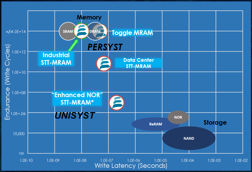
PERSYST and UNISYST for varying memory workloads (Source: Everspin)
Next, we have UNISYST Enhanced NOR SST MRAM, which is targeted at unified code and data memory applications. UNISYST is currently in design.
Also, not shown in the above diagram, we have AgILYST for “innovation and transformation” in the form of configuration bits for FPGAs and Data MRAM for artificial intelligence (AI) neural networks (NNs).
On the one hand, MRAM isn’t the Holy Grail of memories because it lacks the raw capacity of DRAM. On the other hand, although some may see MRAM as a niche market, it’s a niche market that’s growing in leaps and bounds, and Everspin is well placed to take full advantage of the ever-increasing requirements for state-of-the-art MRAM solutions.
What say you? What do you think about non-traditional memory technologies like FeRAM, ReRAM, PCM, and MRAM? And how long do you think it will be before we do discover the Holy Grail of memory?


Mark Twain has said “History doesn’t repeat itself, but it sure does rhyme”.
So now we have magnetic cores in rows and columns instead of capacitors, right ?
Would you care to bet that beancounters will force “Rowhammer”-like crack into these things in the race to highest density no-matter-what ? 🤣🤣
BTW, what is the fundamental difference between MRAM and STT MRAM ? 🙄
I will ask the folks at Everspin to reply to your points and questions.
Their so far only STT MRAM device doesn’t appear to be really DRAM replacement.
Fine, it’s non-volatile (provided that power-up and power-down sequences are honoured) and it doesn’t need precharge time BUT it needs “store time” – 380 ns. Yikes.
It also doesn’t appear to be able to come even close to DRAM’s density, so it loks like they have a long way ahead.
Otherwise it appears to have DRAM or ferrite core mem -like organization – 2D area of cores and one static register “row” for access.
One would expect for them to go for at least some other innovative edge. Like having multiple access (SRAM rows) that one could use for vector operation between rows, pattern searches etc
I understand that they don0t want to step too much outside DDR4 protocol, but given the speeds, i suspect they would most often be connected to an FPGA, which is much more programmable. 🙄
Again, I’ll ask the folks at Everspin to comment — but thanks as always for taking the time to read my columns and ask questions 🙂
Imo all listed schemes miss the mark. They might find their niche, but they don’t look like revolutionary material.
They are simply replay of 60 year old schemes, adapted for microlitography.
In this case, ferrite-beads on a chip scheme.
SImply going for a magnet and a coil instead of a capacitor ain’t gonna solve it. It just replaces one set of problems for another.
Which shows in their products. They’ve got non-volatility, but write cycles suffer. Which makes sense. Magnetized core takes some doing (and time) to remagnetize it.
So, more coercitive materials also need more energy.
And I suspect their density problems come from inter-cell influence. So how do you do magnetic shielding WITHIN a friggin chip ?
MEthinks revolution will come when someone:
-invents transistor-scale element that can do binary logic levels by itself.
– it has control terminals independent of output terminal
– can use some novel quantum effect within its structure to memorize current state.
– doesn’t need a trickle current to keep its state
Playing with MOSFETs and caps should gradually be left to retro tinkerers and overclockers. 🙄
Thank you for the comments on the article about MRAM. I’d like to offer a few responses to the points raised. First, on the fundamentals, STT-MRAM refers to Spin-transfer Torque, which refers to the mechanism by which a magnetic tunnel junction changes its magnetic state. The magnetic state results in a resistive value through the junction, i.e. magnetoresistance, and this is used as the logic data state, “1” or “0” as a memory bit. A previous generation of MRAM used field switching as the way to change the magnetic state, such as in Everspin’s Toggle MRAM. STT is more energy efficient, and more scalable.
On the point of DRAM replacement, it is true that there are DDRx controller implications to be comprehended in system design. But on the larger point of replacing DRAM, that was not the intent for the first couple of generations of DDR3 and DDR4 product introduced. The value of persistence in applications such as enterprise storage write data buffering and to simplify the design of power-loss-protection schemes. The STORE command of 380ns is not a system limiting item since data is stored in the MRAM as you go.. STORE is an option to ensure that all the last writes are persistent, far shorter that completing page writes in NAND or other NV technologies. In terms of density, Our 1Gb ST-DDR4 product is built on 28nm CMOS, DRAM’s are manufactured on specialized, advanced lines tuned to a memory process. That said, new memory technologies introduced have not been replacing previous technologies historically. STT-MRAM is creating new capability for system designers and will complement existing DRAM and NAND technologies. Finally, in terms of going for innovation, we whole-heartedly agree, and that is what is enabling both discrete MRAM as well as innovative ways to use the technology to optimize performance and energy efficiency in AI inferencing applications, so please follow us to learn more as this gets commercialized.
No worries there, I plan to follow you. In the meantime, maybe you could take a moment or three to publish something that could unwrap the fundamentals of working with (STT)MRAM ?
Learned fundamentals of dram since… well since the times of ZX Spectrum, Sinclair QL, Atari ST, Amiga etc.
Which was pretty much from the time of first useable RAMs for mere mortals.
DRAMs back then contained a lot of analogue magic even in its state machine IIRC. It had to, since there was no CLK signal etc.
SInce then, not that much has changed in fundamentals. Yes, we have CLK and instead of jiggling around RAS, CAS etc we have “commands” etc, but underneath there are same limits – one row of SRAM cells and an array of capacitors.
So reading DDR4 or DDR5 protocol specs is not that incomprehensible to me – I can depict what’s ewhat and why it’s there.
Not with this thing. Between all the squirming, my eyes have problems believing that I’m looking at that pdf with right side up.
SO , to spare everyone going through the same datasheet 100x trying to make sense of it, maybe you could do some tutorial ?
Or perhaps the things are in too much of a flux – i.e. you yourself are learning as you go ?🙄