

During its recent quarterly financial update on July 28, Intel announced that it was winding down its Optane Persistent Memory business using what amounts to a footnote in its earnings report. (See “Optane, We Hardly Knew Yeh.”) The writing had been on the wall. There was one fab making production Optane chips based in Lehi, Utah owned by Micron, and Micron sold the fab to Texas Instruments earlier in the year. You can bet that Texas Instruments wasn’t interested in making Optane memory for Intel in Utah. The end of Optane can’t be much of a surprise to anyone.
According to Tom Coughlin and Jim Handy, two of the world’s foremost analysts following the ebb and flow of the semiconductor memory business, Intel has steadily lost money on Optane parts for years – as in many hundreds of millions of dollars per quarter, on average, since 2016. In Pat Gelsinger’s new world for Intel, a product that consistently loses money for years is a product he doesn’t want in his company’s product portfolio.
So Optane ends up on the growing pile of abandoned memory technologies that would challenge DRAM and NAND Flash memory for world domination. Numerous companies have tried to develop many alternative semiconductor memory technologies, and they have all failed to gain significant market share against DRAMs and NAND Flash memory. However, that doesn’t mean that companies won’t continue to try, because the rewards are immense.
Recently, my friend Robert Bielby at Micron told me something that I already knew, sort of, but his framing stopped me short. Of the top four semiconductor companies, three are the leaders in the semiconductor memory business (Samsung, Micron, and SK hynix, which have about 94% of the DRAM market). The fourth company, Intel, invented the semiconductor memory business but then exited, re-entered to make Flash memory, and recently exited again. Wash, rinse, repeat. So, if a company wants to climb to the top of the semiconductor heap, then memory is probably the game to play.
There are several games being played in this market already, and most of these memory technologies involve some sort of non-volatile memory that improves on NAND Flash memory in one or more critical ways. I’ve always been fascinated by the various physical phenomena that semiconductor makers have used to create new, “emerging” types of memory, and there have been more than a few. Coughlin and Handy have summarized these several new and different memory technologies in a new report titled “Emerging Memories Enter Next Phase,” and they have been working on an updated version to cover Intel’s exit from the Optane business. That new version should be available by the time this article appears, so you should check it out.
Many of these new memory technologies may first be used as embedded memory, placed on chip with CMOS logic, but the Holy Grail for all these memory efforts because of the unit volumes involved is the development of “storage-class memory,” which needs to be nonvolatile like NAND Flash memory but as fast as or preferably faster than DRAM so that both existing memory types can be replaced by one new type. That’s a tall order and something to be desired, but not yet attained. Meanwhile, here’s a stroll down the lane of three emerging memory technologies paired with some of my experiences with them.
Ferroelectric RAM (FeRAM, FRAM)
FRAM is the first new memory technology I encountered when I first started to write for electronics publications in the 1980s. According to Coughlin’s and Handy’s report, ferroelectric memory was invented in 1952, the year before I was born. Bell Labs built an integrated 256-bit FRAM array as a monolithic device with no active semiconductor elements in 1955, three years before Jack Kilby cobbled together and invented the first integrated circuit at Texas Instruments. I first encountered FRAM in the late 1980s at a company named Ramtron, located in Colorado Springs. According to Coughlin and Handy, Ramtron did the early commercialization work on FRAM. They write:
“FRAM appears to have sold more unit volume than all other emerging memory types combined. Fujitsu uses FRAM in its RFID chips for subway fare cards and has sold over 4 billion of these chips to date.”
FRAMs exploit a unique physical characteristic of certain crystal lattices. In these ferroelectric materials, an atom can occupy one of two stable places within the crystal lattice. An electric field shifts the mobile atom within the crystal lattice to either one of the two stable positions depending on the field’s polarity and some physical property – perhaps capacitance or resistance – changes depending on the position of that trapped atom.
Four billion chips of any type is a lot of chips, even if it’s used as a subway fare token, so why is FRAM still unknown after all this time and after shipping all those billions of chips? Semiconductor fab managers don’t like ferroelectric materials very much because they incorporate periodic table elements such as lead or bismuth that can easily contaminate the fab. So, FRAM has seen limited use as a non-volatile, embedded, on-chip memory. Coughlin’s and Handy’s report mentions that hafnium oxide and zirconium oxide can also be formulated to exhibit ferroelectric properties, and these materials are already used in fabs for other reasons, so FRAM’s future story is likely to continue.
Resistive RAM (RRAM, ReRAM, Memristors)
In 1971, Leon Chua at the University of California, Berkeley, wrote a theoretical paper titled “Memristor–The Missing Circuit Element.” The paper describes a fourth basic passive electronic device, the memristor, which regulates the flow of electrical current through itself based on the amount of charge that has previously flowed through the device. Chua didn’t build such a device. Back in 1971, the memristor was simply theoretical. It was a hypothetical device that satisfied the apparent need for symmetry in the equations used to describe the behavior of the other three basic passive electronic components: resistors, capacitors, and inductors. Memristors existed in theory, but not in practice.
That all changed nearly four decades later, in 2008, when HP Labs announced that it had managed to build a memristor out of titanium dioxide and that memristors were non-binary devices that could be used to store analog or digital data. It was an electrifying announcement, and people were soon predicting the imminent demise of DRAM, to be supplanted by memristors in the form of resistive memory or RRAM. Further, said HP, it would be using RRAM in its forthcoming moon-shot computer, dubbed “The Machine.”
By 2015, HP had backed off and said it would use DRAM in The Machine instead of memristors. Fifteen years after HP’s memristor announcement, the RRAM revolution has yet to occur, and it doesn’t appear that it will happen any time soon. Coughlin’s and Handy’s report details several RRAM/ReRAM efforts, and RRAM’s time may yet arrive – real soon now, no doubt.
Phase-Change Memory (PCM)
Phase-change memory or PCM uses some major physical transformation of a material – like the transition between a crystalline state and an amorphous state – and the associated changes in electrical characteristics – to store data. Based on its history, Optane memory is likely a type of PCM. Optane’s roots go back to a prolific inventor named Stanford Ovshinsky, who spent decades studying the characteristics and uses for amorphous semiconductors. I remember discussing Ovshinsky’s work with my friend and college classmate Jim Blike back in the early 1970s. He was very excited by Ovshinsky’s pioneering work.
Ovshinsky founded Energy Conversion Laboratories in 1960 to study amorphous materials and their phase-change properties. That lab became Energy Conversion Devices (ECD) in 1964, and one of Ovshinsky’s many innovations was Ovonics Phase-Change Memory, named for himself. Intel and Micron eventually became involved with Ovshinsky and ECD, licensed the Ovonics Phase-Change Memory intellectual property, and announced 3D XPoint PCM in 2015 to much fanfare.
Micron and Intel expended a lot of effort on and generated excitement about 3D XPoint PCM, but I seem to remember that one of the early problems reported with the technology was that moderate heat could anneal the bits right out of a PCM memory cell, and there’s plenty of heat available inside of a data center server. This heat problem meant that PCM might need to be refreshed like DRAM. Depending on how hot the ambient temperature was, the refresh cycles might need to be fairly frequent, on the order of a few seconds. However, I haven’t heard much about this problem lately, so perhaps it’s been solved.
The problem that has not been overcome is the relative cost per bit. Intel’s losses on Optane memory devices and Micron’s prior exit from the 3D XPoint venture stand as proof that even major semiconductor makers like Intel and Micron have great difficulty making PCMs price competitive, even with a decade of R&D behind the effort.
Magnetic RAM (MRAM)
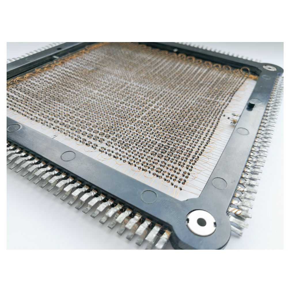
I must confess, I have a special affinity for magnetic memory. The first computer to use magnetic memory was the MIT Whirlwind computer project, which got the world’s first magnetic core memory on August 8, 1953, just a month before I was born. Magnetic core memory completely dominated the computer memory space for the next two decades. However, Intel’s introduction of the first commercially viable semiconductor DRAM, the 1103, in late 1970 sounded the death knell for magnetic core memory.
Core memory had remained a hand-woven and therefore expensive product. It resisted every effort to automate its manufacture, although companies did try. They simply failed. Meanwhile, semiconductor DRAM leveraged the mass-production manufacturing technologies that made integrated circuits the driving force in the electronics industry, starting with lithography. Magnetic core memory vanished seemingly overnight. By 1975, DRAM clearly ruled the memory roost.
Magnetic memory has continued to fascinate technologists over the years. Intel, Western Electric, Texas Instruments, Rockwell, National Semiconductor, Hitachi, Westinghouse, Motorola, Fujitsu, and Sharp all made failed attempts to commercialize magnetic bubble memory starting in the late 1970s. IBM developed Racetrack memory, an updated, 1-dimensional version of bubble memory, starting in the early 2000s. Still not there yet. Even if one of these magnetic memory technologies succeeds, they’re serial memories and therefore relatively slow and good only for disk replacement or, these days, for replacing SSDs based on NAND Flash memory.
Magnetic RAM, MRAM, attempts to meld the mass-manufacturing techniques of lithography-based semiconductor production with magnetic bit storage. Nonvolatile MRAMs are now available as commercial products from Everspin Technologies. I have been writing about that company for at least ten years. Everspin says it has sold many millions of its MRAM chips. That’s nowhere close to DRAM and NAND Flash unit volumes, but it’s not nothing, either.
However, MRAMs have two significant competitive problems compared to DRAM and NAND Flash chips: bit density per chip and cost. MRAM vendors are trying all sorts of ways to overcome these competitive challenges. The latest hope is called STT (Spin Torque Transfer) MRAM. Coughlin’s and Handy’s report provides vast amounts of technical detail for nine different types of MRAM, including STT MRAM.
Perhaps one of the four types of emerging memory – FRAM, RRAM, PCM, or MRAM – will be the Holy Grail for Storage Class Memory. Perhaps it will be some other memory technology. Maybe something like Star Trek’s isolinear chips, whatever they are. Time will tell.


It seems the best new memory technology would be one that eliminates the need for program storage memory. A Flowpro Machine models with software and produces hardware for that software model. No program storage.
In U.S. Patent 2,268,872 dated January 6, 1942, W. R. Hewlett describes and claims the analog use of a memristor to control the oscillation amplitude of a resistance-capacitance vacuum-tube audio oscillator. Hewlett used a small incandescent lamp as a short-term memory-resistor, though he did not use the word memristor.