


STMicroelectronics (ST) and GlobalFoundries (GF) have just signed a memorandum of understanding to create a new, jointly operated 300mm semiconductor fab to be located alongside ST’s existing fab in Crolles, France. The new fab will support multiple semiconductor technologies and process nodes, including FD-SOI (fully depleted silicon on insulator). ST and GF expect that the fab will start producing chips in 2024 and will ramp to full capacity, producing as many as 620,000 300mm wafers per year, by 2026.
The Grenoble area in southeastern France, not far from the Italian border, has long been a hotbed of FD-SOI development. In many ways, FD-SOI is a lower-tech approach to realizing some of the benefits of FinFETs and gate-all-around FETs (GAAFETs) – including higher speed, lower power consumption, and less parametric variation on a chip from transistor to transistor thanks to the conduction channel being fully depleted (undoped). Less on-chip parametric variation means that IC designers can reduce the amount of design margin needed – for both supply voltage and timing – which improves the chip’s speed and lowers its power consumption by lowering the required operating voltage.
Dr. Chenming Hu and his team at the University of California, Berkeley, developed FinFETs way back in 1999 under a DARPA contract. DARPA cut that contract because it was clear that planar FETs would eventually run out of gas after their half-century run as they were scaled smaller and smaller. DARPA sought an alternative.
Small planar FETs suffer from short-channel leakage, which prevents the FET from turning off completely. The advantage that FinFETs have over planar FETs is that the FinFET architecture constructs a gate around three of the FET channel’s four sides. This arrangement allows the electric field from the gate to penetrate more deeply into the FET’s conduction channel, which reduces short-channel leakage and allows better control over the current through the channel.
Short-channel leakage increased in magnitude as planar FET dimensions shrunk, causing power consumption and heat-dissipation challenges to grow and forcing semiconductor makers to adopt FinFETs. Intel was the first commercial semiconductor company to adopt FinFETs for its 22nm process node back in 2011, more than a decade after FinFETs were first developed. FinFETs are currently used almost universally for chips made with 20nm process nodes or newer.
However, FinFETs are now running out of gas. Driving three sides of the FinFET transistor’s gate no longer achieves the desired speeds and low leakage currents. We must now drive all four sides of the FET gate to get a well-behaved transistor. Enter GAAFETs, which are already in production at Samsung’s fabs in that company’s 3nm process node. Intel and TSMC will also be using GAAFETs for their Intel 20A and N2 2nm nodes respectively. Samsung calls its GAAFETs “Multi-Bridge-Channel FETs” (MBCFETs); Intel calls them “RibbonFETs”; and TSMC calls them nanosheet GAAFETs. (See “Intel Welcomes You to the Angstrom Era” and “Moore’s Law: Not Dead Yet? Nope, Says Intel:, Behold Intel 4… and 3.”)
Like FinFETs, GAAFETs are 3D structures. Instead of fins, GAAFET conduction channels are built with undoped silicon nanowires, nanosheets, or ribbons that are so thin that they are essentially 2D structures, made with advanced process technologies such as atomic layer deposition (ALD). These nanoscale conduction channels are entirely encapsulated by the GAAFET’s gate structure.
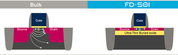
The ultra-thin conduction channel of an FD-SOI FET does not suffer from the same leakage effects as a planar FET made in bulk silicon. Image credit: STMicroelectronics.
FD-SOI FETs have what is essentially a 2D conduction channel, created by bonding or otherwise applying a very thin, extremely uniform layer of silicon on top of a thin, grown silicon dioxide insulation layer. If the FD-SOI FET’s conduction channel is thin enough, the electric field from the transistor gate sitting on top of the conduction channel fully penetrates the channel, thus eliminating the need for a gate structure that surrounds the channel on all four sides, as is done with GAAFETs.
Except for the FD-SOI substrate, FD-SOI FETs are made in a similar manner and with the same equipment used to make planar FETs. The GAA structure is more complex and requires the use of expensive EUV lithography to create the small structures required. Like FinFETs and GAAFETs, FD-SOI FETs do not suffer from short-channel leakage problems, and they don’t require EUV lithography as do GAAFETs. So, you might call FD-SOI transistors “gate-almost-all-around FETs” (GAAAFETs). You might, but no one does.
By an interesting coincidence, the same UC Berkeley team – led by Dr. Chenming Hu – that developed the FinFET under a DARPA contract in 1999, simultaneously developed something very much akin to the FD-SOI FET architecture under the very same DARPA contract. Hu dubbed this second FET structure UTBSOI (Ultra Thin Body Silicon on Insulator).
FinFETs, GAAFETs, and UTBSOI FETs offer many benefits over planar MOSFETs:
- Better signal swing
- Less sensitivity to gate length and drain voltage
- No random dopant fluctuations because the FinFETs fins, the nanostructured conduction channels in GAAFETs, and the thin conduction channel in UTBSOI/FD-SOI FETs are all fully depleted – they’re not doped
- Higher on current with lower leakage
- Lower Vdd and lower leakage, therefore less power consumption
There are at least two important differences between FinFETs or GAAFETs and UTBSOI/FD-SOI FETs. First, it’s relatively easy to add back biasing beneath the channel of an FD-SOI FET, a capability that’s enabled by the bulk silicon substrate under the thin insulating layer on the wafer. Back biasing allows you to play with FET threshold voltages and to tweak performance and power consumption. If you decide to get really fancy, you can tweak individual FETs on the chip by using the silicon under each transistor as a second gate. There’s no easy way to add back biasing to FinFETs or GAAFETs. Second, you don’t get smaller transistors with FD-SOI relative to FinFETs or GAAFETs, so you don’t achieve the same transistor densities. That’s the flip side of not requiring expensive EUV lithography.
FD-SOI processing is still more expensive than conventional planar IC processing because it requires special FD-SOI wafers. It’s just not as expensive as the EUV lithography and other 3D processing techniques needed to make small FinFETs and GAAFETs. Conventional IC manufacturing uses bulk silicon wafers, which are much less expensive than FD-SOI wafers. The major supplier of FD-SOI wafers is Soitec in Bernin, which is literally just down the street from the STMicroelectronics Crolles fab complex north of Grenoble.
By coincidence, Soitec, GF, and ST, along with CEA (the French Alternative Energies and Atomic Energy Commission), announced a collaborative agreement earlier this year to jointly define the industry’s next generation roadmap for FD-SOI. In that announcement, CEA Chairman François Jacq said, “CEA has… a long history of deep R&D cooperation with… STMicroelectronics, Soitec and GlobalFoundries and has been very active in the initiatives led by the European Commission and Member States aiming to set up a complete ecosystem for FD-SOI going from material suppliers, design houses, EDA tools providers, fabless companies, and end users.” These are the elements that constitute an FD-SOI “platform.”
July’s ST/GF FD-SOI memorandum announcement also says, “ST and GF will receive significant financial support from the State of France for the new facility. This facility will strongly contribute to the objectives of the European Chips Act, including the goal of Europe reaching 20% of worldwide semiconductor production by 2030.” This statement was a European poke in the eye for the US government, which appeared to be dragging its heels on the country’s own CHIPS Act, much to the chagrin of companies such as Intel and TSMC. However, the US Senate and House of Representatives finally passed the bill last week and US President Joe Biden is expected to sign it into law this week.
It appears that France is going big on FD-SOI, which is not a bad strategy if you don’t plan to buy a $150 million EUV stepper or the next-generation $300 million “High NA” EUV stepper from ASML. FD-SOI confers many of the FinFET’s and GAAFET’s advantages on a far less expensive process node. GF already offers two FD-SOI process nodes or platforms called RF SOI and 22nm FDX22. (See “GlobalFoundries Chases Down a Different Semiconductor Rabbit Hole.”) In May, GF announced an RF meta platform called GF Connex that rolls together elements of the company’s RF SOI, FDX, SiGe, and FinFET semiconductor platforms to meet the varied communications needs of smart mobile and IoT devices and communications infrastructure equipment.
For its part, ST currently offers a 28nm FD-SOI process/platform. The 28nm node is currently the most cost-efficient process node in the industry, so there are a lot of economic benefits to staying with this node. However, technology inevitably marches on, and the Crolles joint announcement mentions an 18nm ST process technology. This appears to be the same 18nm FD-SOI process technology with embedded PCM (nonvolatile phase-change memory) that Orio Bellezza – President, Technology, Manufacturing, Quality and Supply Chain at ST – discussed during his STMicroelectronics Capital Markets Day presentation titled “Technology and Manufacturing” in May of this year.
The joint announcements by ST, GF, and CEA bolster FD-SOI’s position as a viable alternative to GAAFETs for the next few decades in specific applications, including applications in the automotive, IoT, and mobile markets. For these applications, it’s not the sheer number of transistors that’s important; it’s what those transistors can do.
For more information about the various semiconductor foundry platforms GF currently offers including the 22nm FD-SOI platform called FDX, see “GlobalFoundries Chases Down a Different Semiconductor Rabbit Hole.”


One thought on “STMicroelectronics and GlobalFoundries Jointly Press on with FD-SOI in a New Fab Near Grenoble”