


There’s a saying: “Everything stays the same until it changes.” Well, perhaps we need a slightly modified version of this for semiconductors: “Everything stays the same until it has to change.”
OK, so that’s probably not something exclusive to chips – because of a related saying: “If it ain’t broke, don’t fix it.” In other words, change only those things that are preventing you from achieving some goal. Like printing features of the size needed for some process node.
Today we’re going to look at a couple of papers plus an announcement as we cover two – or is it three? – different process nodes. Yeah, you’d think I could count to three pretty much unerringly, but, in this case, it’s not I that am confused: there appears to be a disagreement among authors as to what belongs in a given process node.
Both Intel and GlobalFoundries had silicon platform papers at last December’s IEDM conference, and, though featuring different improvements, they both reported similar results. (Some numbers higher for were Intel, others for GlobalFoundries.) Here’s the thing, though: Intel referred to theirs as a 10-nm process, while GlobalFoundries called theirs a 7nm process. Who’s right? We’ll come back to that in a minute. Let’s start by looking at the improvements that each company featured.
Intel’s Take
Intel speaks of using a third-generation FinFET in their “10nm” node, patterned using self-aligned quadruple-patterning (SAQP). They’re leveraging cobalt for the local interconnect (and contacts), which they say gives them a 60% reduction in contact line resistance. And they’ve saved layout space in a couple of different ways.
In current platforms, the contact for the transistor gate is laid out to the side of the active areas of the transistor; this takes extra space. Intel moved the contact to be over the diffusions, making the cell smaller.
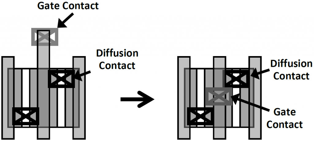
(Image courtesy IEDM)
More savings came from a change to the edge of cells. Their existing platform requires a dummy gate at the edge, which uses up precious space. In the new work, they’ve taken out that requirement and put in an isolation trench along the edge instead.
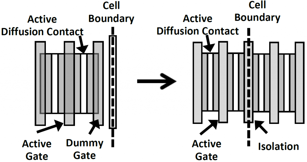
(Image courtesy IEDM)
In addition, they say that they’ve improved transistor matching to the point that fewer fins can be used – a clear space-saver.
The fin has grown taller: 46 nm tall. With a width of 7nm, that’s almost a 7:1 aspect ratio. Other top-level bullet points include what they call fifth-generation high-Κ metal and seventh-generation strained silicon, 12 metal layers, and an ultra-low-Κ dielectric between metals. They claim 2.7x scaling over the 14nm node.
Other improvements:
- The source and drain diffusions are raised, and they’ve added a titanium layer that wraps around those regions to lower the spreading resistance.
- They use a low-Κ spacer, lowering the gate-to-contact capacitance by 10%.
- They achieve undoped fins using 4-6 work-function metals for low-, standard-, and high-VT devices.
It’s worth noting the value of the undoped fin, since, as we’ll see, Intel isn’t the only one doing that. By setting the threshold using work-function metals instead of fin doping, they get better channel mobility (none of those pesky dopant atoms cluttering the straightaway), they get better PMOS and NMOS matching, and they do away with the whole issue of random dopant variation, since the number of dopant atoms would be so small.
We’ll come back to look at some of the pitches they achieved in a moment.
GlobalFoundries’ Take
GlobalFoundries also claims a third-generation FinFET – in their “7nm” platform. They’ve built the process assuming 193i lithography, with SAQP for the fins and SADP for backend metal. That said, they’ve also planned for EUV insertion as an option to replace the multi-patterned layers. Designs done for 193i would naturally need some new masks to move to EUV, but they say that no design changes would be required.
They’ve also architected the dimensions such that basic logic can be implemented with two-fin transistors, while designs targeting the high-performance computing (HPC) space can accommodate four-fin devices.
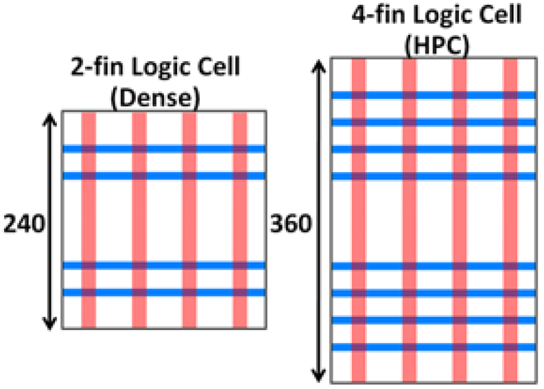
(Image courtesy IEDM)
Overall, they’re claiming 2.8x scaling over the 14nm node – roughly the same as what Intel is claiming with their “10nm” node. They also claim greater than a 40% speed-up over 14nm (at fixed power) or a 55% reduction in power (at fixed speed).
They’ve also done an undoped fin by using work-function metals to provide “RVT,” “LVT,” and “SLVT” transistors, plus an “XLVT” version for HPC.
Additional improvements include:
- Careful fin shaping and profiling for reduced short-channel effects.
- Junction/epi optimization.
- Contact resistance optimization, including the use of cobalt for the middle-of-line (MoL; contacts, local interconnect)
10nm vs. 7nm
So, to get a sense of the difference between Intel’s “10nm” node and GlobalFoundries’ “7nm” mode, we can build a table that stacks up some of the numbers.
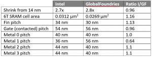
In other words, most parameters end up pretty darn close. (Comparison of the shrink from 14nm assumes they both mean the same thing with the 14nm designation.) Yes, there’s one outlier – metal 1 pitch – and yet, in that case, Intel’s 10nm process is more aggressive than GlobalFoundries’ 7nm version.
I asked both companies about how they named the node. Intel’s lead author, Chris Auth, said,
“I get this question a lot. Node names across the semiconductor industry have lost much of their meaning over the past 10 years.
“Intel has tried to follow historic trends and use node names that indicate ~0.7x linear scaling and ~0.5x area scaling for each generation (e.g. 22nm is 0.7x of 32nm). However, Intel’s recent 14nm and 10nm generations have each provided better than 0.4x area scaling due to aggressive scaling, so Intel node names are clearly conservative and don’t reflect the true area scaling benefit moving from node to node.”
GlobalFoundries had the following comment:
“We… feel that when comparing process nodes, it’s important to consider more than just transistor density. For instance, cost and complexity are two critical factors that are not considered in typical density metrics. Likewise, the timing of introduction is also important. The pure-play foundries have been accelerating their introduction of leading-edge nodes, while IDMs have been slowing down their cadence.
“While node names no longer directly correlate to physical dimensions, they do represent a relevant benchmark for the industry. Increasingly, our customers are more concerned with system-level PPAC characteristics than the number and type of transistors on a chip. GF’s 7LP provides a full node scaling and more than a node of performance from foundry 14nm/16nm, and, therefore the naming is a reflection of the PPAC benefit to the customer.
“For GF, node transitions are a way to convey generational improvements that are in line with historical performance expectations that can justify a move to a new process technology.”
So, yes, this would seem to be a particularly stark illustration of the… well, if not arbitrary, then at least confusing, nature of the node-naming process now that it’s lost touch with any physical parameter as justification. I’m not qualified to adjudicate who’s right or wrong… It’s just… confusing.
So… on that note, let’s jump a node and see what’s happening way out in the future.
Cadence and Imec on 3nm
After 7nm comes 5nm, right? And after 5nm comes 3nm. Except, see above: it’s not that cut-and-dried. You’ll see references to a “7+” node; Samsung has a 4nm node in the works (having also discussed 8 and 6nm nodes). Some will argue that there are meaningful differences in these node numbers; others will argue that they’re now driven by marketing. What’s certain is that it’s hard to know whether comparing two technologies at the “same” node level means comparing apples and oranges.
One bit I’d heard mentioned in the past was that new transistor configurations – like nano-wire channels with gate-all-around (GAA) structures – would make their appearance at the 5nm node. That appears not to be the case from what I’ve seen more recently (and from what Applied Materials said with respect to replacement-metal gates).
So will GAA show up at the 3nm node? Even that’s not clear, at least according to Imec and Cadence, who just announced the tape-out of a 3-nm test chip. This reflects early stages of exploration, and they’re looking at tall-fin FinFETs, GAA nano-wire transistors, and GAA nano-sheet transistors (such as are proposed in Samsung’s 4nm platform).
The whole idea with GAA transistors is that you have the channel completely surrounded by the gate, giving better control. With a tall FinFET, you have all but the bottom footprint under control, so making it tall reduces the proportion of surface area not contacted by the gate. The good news with GAA is that there is no uncontacted area. The bad news is that it’s new, uncharted ground. And this is where it’s particularly clear that there will not be a change unless it’s absolutely necessary.
They see metallization moving from copper to something else – possibly cobalt. The problem here is with the plating technique used to deposit the copper today; there’s a minimum for the area that can be plated, and 3nm will go below that minimum. It really seems to be the process more than the specific metal that’s the issue, since whatever would be used would likely be deposited using chemical vapor deposition (CVD). Looking around, there would appear to be work underway on copper CVD (at least as of a couple years ago, although much of what’s out there dates to the early 90s). Presumably, if copper CVD can work out, then there may be a battle.
Another transition coming sometime even further in the future is the move to 3D, and this comes in two independent ways. One involves flipping the transistor channel vertically using what Imec calls a VFET (and what I’ve liked to call a PinFET – although it turns out this term is already taken for P-intrinsic-FETs). The second 3D move is to stack layers of transistors atop each other – either full circuit layers or the stacking of n-type and p-type transistors atop each other for a CMOS pair, referred to as a CFET. Imec and Cadence see these more likely happening at the 2nm node.
That last one, stacking layers, might sound mechanically straightforward, except that there are two thermal issues. The first involves fabrication. It’s a known thing that back-end process steps need to go easy on the temperature so that they don’t change how materials like dopants are positioned within the silicon.
With a single transistor layer, that’s easy (-ish). But with a second layer, now, once you’re done with the first-layer front-end, you don’t move to the back-end; you have another layer of front-end. Will that mess up the first layer? Or do you derate the high-temp operations on the first layer knowing that more high temp steps are coming? Complicated stuff.
The second thermal issue involves getting the heat out between multiple layers during operation. Will a first-layer transistor heat things up and change the second-layer transistor’s behavior? How do you simulate that, since the transistors may not be operating 100% of the time?
This is an old, well-known issue that probably won’t be solved until it has to be.
Because, just as we’re seeing with FinFETs and copper and single-layer design, we all know that everything stays the same until it has to change.
More info:
Intel 10nm platform: IEDM 2017 proceedings, paper number 29.1
GlobalFoundries 7nm platform: IEDM 2017 proceedings, paper number 29.5


What do you think about these platforms? And the nodes they’re named after?
Something is wrong with data in the “6T SRAM Cell Area” row, either the data has been swapped between the Intel and GF columns or the ratio should be 1.16 not 0.86.
You’re right! Good catch; thanks. Updated to fix it.
its great. but what does it all mean for consumers? the transition from finfet to GAA
the annual 5% increase in synthetic work?