

There’s a problem with transistor gates at 5-nm and below. There’s simply not enough room for all the things in the metal stack used for contacting the gate.
Let’s break that down, at least from the viewpoint of Applied Materials as described to me (and presented) at last fall’s IEDM show. In a simpler world, you’d have a gate metal, and it would touch the gate, and that would be that. But noooooo… that would be too easy. Let’s work our way through the stack.
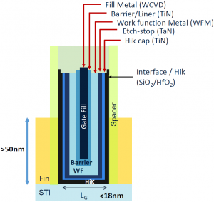
(Image courtesy Applied Materials)
The thing is, the structure is that of a high-aspect-ratio (HAR) trench that needs to be filled with lots of stuff. We start with the high-Κ material, HfO2. That allows us to influence the channel over a thicker dielectric layer than if we used SiO2. Then that layer is capped with TiN. This is followed by an etch-stop layer of TaN. After that come(s) the work-function metal layer(s).
At that point, we should be ready for the fill metal that will close the trench. Except for one thing: we’re using tungsten (W) as fill, applied by chemical vapor deposition (aka WCVD). And the tungsten precursor is WF6. That’s all well and good, except that we want tungsten metal in the end, not some fluoridated version. Which means that the WF6 must dissociate in the deposition process, liberating fluorine. And you don’t want that to diffuse into the stack.
So you need a TiN barrier layer – and a thick one at that – to keep the fluorine from contaminating the work-function metal. We need to lay that barrier down before we can finally put in the fill metal. Which brings up a second problem.
The tungsten fill arrives as a conformal coating, growing from the edges in. That means that, in a HAR feature, the fill will grow from the sides and meet in the middle, leaving a seam. If the trench is “re-entrant” – meaning that it’s wider inside than at the opening, then the opening may close off before the inside is full, leaving a void. Suboptimal. AKA, not good.
But here comes the biggest problem. It’s one of arithmetic. And it comes from the desire to provide transistors with different thresholds. This is done by varying the thickness and type of the work-function metals. In a so-called “PMOS-first” configuration, the p-type work-function materials will be laid down selectively over the PMOS gates, and then the n-type materials go on over all gates. So the PMOS devices are already burdened by two sets of work-function metals. And the low-VT devices have the thickest of the layers.
So here comes the arithmetic part. Note that the length of the gate above is 18 nm or less. That means that all the metals in the sideways stack meet in the middle at 9 nm. Let’s look at that more closely.
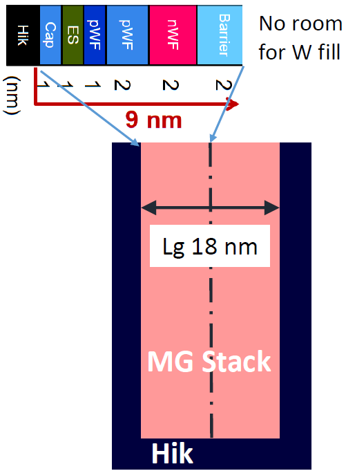
(Image courtesy Applied Materials)
We usually look at the stack vertically, but, along the sidewalls, it stacks up horizontally due to conformal coatings. And what you see above is the low-VT PMOS stack for a PMOS-first flow. You may notice that there’s no fill. In fact, if you have a keen eye, you’ll notice the lack of a hard line “above” the barrier – because there’s not even room for the entire thick barrier. (I suppose that doing the NMOS work-function metals selectively would also remove some height, but I’m going to assume that costs too much…)
This is where Applied is proposing a change to the metal used in the fill. Instead of tungsten, they’re going with cobalt. They won’t say what the precursor is (they consider it intellectual property), but, notably, it doesn’t involve fluorine. So, while a barrier is still needed, it can be much thinner, relieving the congestion in the trench.
But replacing one metal with another cannot be done willy-nilly. Will cobalt perform as well as tungsten? Cobalt isn’t completely new in the semiconductor world; Applied also proposed it for via fill several years ago. But this is the extra-sensitive gate, a place that is likely to garner an if-it-ain’t-broke-don’t-fix-it attitude.
So Applied has looked closer at how it performs over the gate. If you look at just bulk resistivity, it’s not obvious that cobalt would beat out tungsten: tungsten has a resistivity of 5.4 µΩcm, while that of cobalt is 6.34 µΩcm. So tungsten would appear to conduct better.
But what about these metals in a thin film? In that kind of application, granularity matters a lot more, and the top and bottom closing in means more scattering and what not. So, for instance, the resistivity of tungsten in a 15-nm (or so) thin film shoots up from 5-point-something to 36 µΩcm. What about cobalt?
Applied found that cobalt in thin doses as laid down using their reflow process still maintains a bulk-like resistivity under 10 µΩcm. This is partly assisted by the fact that the grains end up being large, which keeps resistance lower. And it means that you can get away with a thin fill layer without killing conductivity. So now you have both a thin barrier and thin fill metal that conducts better.
The reflow process also isn’t conformal, so you don’t get the seam – or even voids – in the trenches. This further boosts conductivity.
You could think of this as adding yet another metal to the process, except that you might already be using cobalt for vias. You’re obviously not going to be combining steps, since the gate is a front-end step, while vias are back-end steps.
In addition, the via process from a few years ago uses CVD for depositing the cobalt, much as is done for tungsten with gates today. Which, for the gates, would lead to the conformal issue with seams and voids. So doing the gate cobalt by reflow instead of by CVD is an important distinction.
One last note here, since we’re talking about the 5-nm node. I’ve heard talk about this possibly being the node where we move from FinFETs to nano-wire gate-all-around (GAA) transistors. Which got me wondering whether the specific application targeted by this technology applies as well to GAA. It’s not obvious that it would.
Applied replied that the foundry implementation of 5 nm will be through scaling the FinFET structure down, not through GAA. They see GAA coming, but they don’t have good visibility into which node will take on that new transistor.
More info:


What do you think about AMAT’s approach to gate metal for aggressive-node FinFETs?