


As you may have gathered from my recent Logic Diagrams and Machines column, I spend more time than perhaps I should cogitating and ruminating on the past, pondering the imponderable and effing the ineffable. One of the topics I often contemplate is what would happen if I inadvertently wandered into a timeslip and found myself transported back to the late 1930s or early 1940s (my uncle was never the same after it happened to him).
We discussed some of this earlier in my Building a Computer, Should You Inadvertently Travel Back in Time column. Also of interest is my ongoing Heath Robinson Rube Goldberg (HRRG) 4-Bit Mixed-Technology Computer project. And, while we’re here, I would feel foolish to miss out on the opportunity to remind anyone who might be in a position to make my dreams come true that I would be more than Willing to Provide Good Home to IBM System/360 Front Panel.
One topic that intrigues me is that of the various flavors of computer memory with which the ancients experimented before semiconductor versions came to the fore. I think we could argue that water-based capacitors provided a form of memory in the Monetary National Income Analogue Computer (MONIAC), which was created Down Under in 1949. As a point of interest, MONIAC was the inspiration for the Glooper (a.k.a. “The Thing in the Cellar”) found in Terry Pratchett’s Discworld universe. Similarly, as discussed in an article from 1964, electronic capacitors could be used as memory elements for electronic analog computers. Now I’m wondering if there are any analogues for mechanical analog computers.
In the case of digital computers, Konrad Zuse’s mechanical Z1 computer had a purely mechanical digital memory (this painstakingly handcrafted binary, floating-point machine was up and running circa 1938 in Berlin, just in time to get blown up in WWII). Later digital machines used a variety of techniques to implement memory systems, including rotating capacitive and magnetic drums, vacuum and Williams tubes, relays, and mercury delay lines, to name but a few.
Perhaps it’s because I enjoy blowing bubbles (who doesn’t?), but I always had a soft spot for those small but feisty magnetic bubble memory modules that graced us with their presence for too short a time. And don’t get me started on the topic of bulk storage in the form of perforated paper products (cards and tapes), magnetic tapes, and magnetic-based hard disk drives (HDDs).
Eventually, of course, we developed semiconductor memory devices in the form of SRAM and DRAM, EPROM and EEPROM, and Flash. There are other contenders, including phase-change memory (PCM, a.k.a. PRAM), magnetic RAM (MRAM), ferroelectric RAM (FRAM or FeRAM), resistive RAM (ReRAM), and that’s just for starters, but let’s not wander off into the weeds.
Out of all the above, the three main technologies are SRAM, DRAM, and Flash. Both DDR (double data rate) in all its incarnations and HBM (high bandwidth memory) are based on DRAM. Meanwhile, Flash comes in two main flavors: NAND Flash and NOR Flash.
Based on their mistaken belief that NOR Flash was on the way out, a lot of manufacturers decided to exit the arena around a decade ago. Unfortunately, they made their move too soon, because more and more applications and markets started to take advantage of the advantages offered by NOR Flash. As a result, by 2020, the folks at Macronix, who had kept the NOR Flash faith, found themselves leading the NOR Flash market with a 24% share. Even better, this is a market that’s experiencing a boisterous CAGR of around 15%, which is anticipated to last until 2025 and beyond. And, better yet in these trying times is the fact that the folks at Macronix perform all their wafer manufacturing in-house using their own 200mm and 300mm fabs (the lucky scamps).
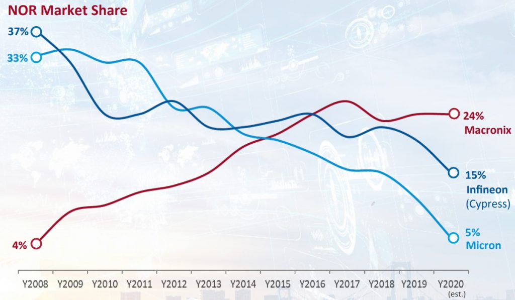
By 2020, Macronix had established a leading position in the NOR market
(Image source: Macronix, Data Source: Omdia (iHS Market) and Macronix Marketing)
So, is NOR Flash better than NAND Flash? Hmmm, the answer is “Yes,” “No,” or “Maybe,” depending on what you wish to do with it. I should also point out that the folks at Macronix offer both NOR and NAND products, so they have no axe to grind either way (well, apart from the fact that they are market leaders in the NOR Flash department LOL).
To summarize things in a crunchy nutshell, NAND Flash has a much smaller cell size, much higher write and erase speeds, and comes in much higher capacity/density components than its NOR Flash cousins. By comparison, NOR Flash offers true random access coupled with much faster read speeds, thereby making it ideal for executing code. Also, NOR Flash is more reliable and better at retaining data than its NAND Flash counterparts.
As I wrote in my NOR Flash is Sexy Again! column, “The NAND and NOR forms of Flash each have their own advantages, disadvantages, and preferred application arenas. In particular, NAND Flash finds favor in bulk data storage deployments, whilst NOR Flash shines when it comes to code storage and execution tasks.”
The key points here are that users love the fast access times of NOR Flash (~100ns for NOR flash vs. ~100us for TLC NAND Flash), they love the simplicity (simple SPI interface vs. NAND Flash’s reliance on a complex controller), and they love the fact that they can get automotive grade NOR Flash.
So, with all this love in the air, what’s the problem? Well, as always, users aren’t satisfied with what they currently have (bless their little cotton socks) and they want higher capacity NOR Flash devices. The issue here is that existing 2D Flash technology is limited with respect to scalability.
All of which leads us to the fact that I was just chatting with Anthony Le, who is VP of marketing for Macronix America, Inc. Anthony informed me that the guys and gals at Macronix are in the process of extending their 2D NOR Flash offerings by leveraging their proven experience with 3D NAND to create a suite of next-generation 3D NOR devices.
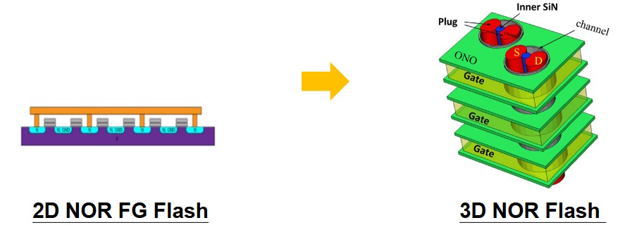
Transitioning from 2D NOR to 3D NOR (Source: Macronix)
It’s important to note that when we say 3D, we are talking about a 3D process stacking technology, NOT a 3D die stacking technology. The folks at Macronix currently have a 32-layer 3D NOR Flash line in development that will provide 7x the memory density of 2D NOR Flash. In the future, Macronix may further extend the density by using hundreds of layers. Like their existing 2D NOR Flash counterparts, these 3D NOR Flash devices will be available in industrial and automotive (AEC) grades.
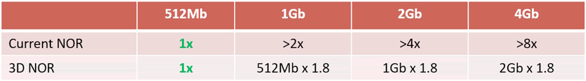
Initial pricing strategy (Source: Macronix)
What does all this mean in real, nitty-gritty terms? Well, consider the initial pricing strategy table above. The “Current NOR” row refers to existing 2D NOR Flash.
The idea here is to provide a cost-effectiveness comparison between 2D and 3D NOR Flash. The 1x for current 2D NOR Flash is normalized. It doesn’t matter which vendor you are talking about (Macronix, Micron, Infineon). As an example, I just bounced over to Mouser and found a 512Mb NOR flash for ~$1.
If you want a 1Gb NOR Flash using existing 2D technology, you will have to stack two 512Mb 2D dice, which means 2x the cost. The reason the table shows “>2x” is that there’s also a cost associated with die stacking, but we are focusing on the cost of the silicon here. Similarly, a 2Gb NOR Flash will require a stack of four 512Mb 2D dice (4x the 512Mb cost), while a 4Gb NOR flash will require a stack of eight 512Mb 2D dice (8x the 512Mb cost).
By comparison, when using 3D NOR, everything is implemented on a single die. This is why Micronix has an initial pricing strategy as shown. A 1Gb die will be priced at 1.8x a 512Mb die, a 2Gb die will be priced at 1.8x a 1Gb die, and a 4Gb die will be priced at 1.8x a 2Gb die. Also, there are no additional die stacking charges because… well… we aren’t stacking die. Assuming $1 for a 512Mb 3D die, then a 4Gb die will cost $1 x 1.8 x 1.8 x 1.8 = $5.80 (as opposed to $8 for a stack of eight 512Mb 2D dice). Remembering how avidly automotive manufacturers count their pennies; I can only imagine how their eyes are going to light up when they hear about this.
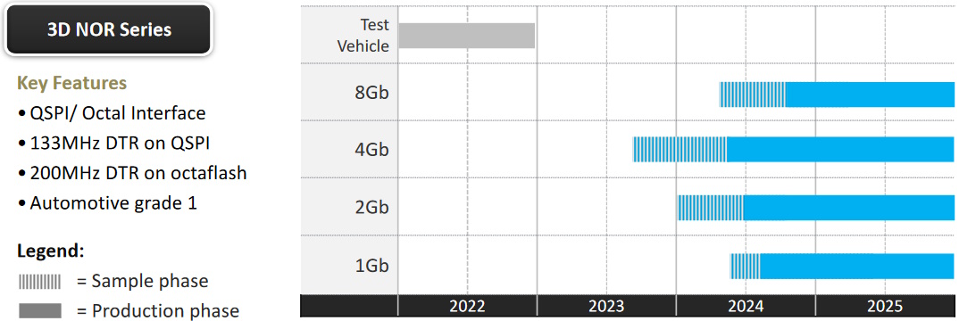
3D NOR Flash product plan (Source: Macronix)
I know what you are thinking: “Enough of the waffle already! When will I be able to lay my sweaty hands on these little beauties?” Well, the above chart reveals all. Of particular interest is the fact that the 4Gb parts are sampling as I write these words and as you read them.
Anthony closed by saying how much he’d enjoyed my NOR Flash is Sexy Again! column, and he pointed out that “NOR Flash just got even sexier.” I mean to say… seriously? It’s not often that the person giving me a briefing for a column also drops the title for that column in my lap. How about you? Do you have any thoughts you’d care to share on anything you’ve read here?


I know zip about the technology, but I am convinced that the computer evolution will be to use of memory blocks instead of ICs for computation as well as control and storage.
And it is only a small step away.
We all have gigabytes of memory… I would like to point out that NASA Houston control center had a cluster of 4 System360/Mod75 computers, each with — watchout — ONE megabyte of memory! and they put a man on the moon round trip. There was also a shared storage memory of maybe another megabyte.
All of the System360 except the Mod75 and Mod91 were microprogrammed control. Just that the arrays were not big enough and fast enough? for these models.
And the 360 follow ons have all been microprogrammed, including Z.
Now according to “Amelia’s Fish Fry” AI needs a new breed of computer and I say “build it out of memory blocks!”
I didn’t get to talk about it here — but Macronix do have in-memory compute capability — also a lot of folks are working on Computational SSD or Near Data Processing (NDP) where a lot of processing actually takes place in the drive. One day we will have a memory that has all of the advantages (and none of the disadvantages) of SRAM, DRAM, MRAM, FeRAM, PRAM, and Flash … and when that glorious day comes….