


At this year’s Semicon West show, Soitec made a presentation summarizing the state of the union with respect to silicon-on-insulator (SOI) technology. We’ve looked at FD-SOI a couple of times, particularly with respect to GlobalFoundries’ implementations at 22 and 12 nm. But today we’re going to look more generically at the technology – and the fact that there are various extant flavors of SOI and that that will continue. (We’ll return to GlobalFoundries in a future piece.)
The major take-away for those of us more focused on logic design is that FD-SOI is a recent addition to the SOI family (relatively speaking). Turns out that RF-SOI is, at present, about 60% of SOI sales. Who knew! And Power SOI is another 20%.
The non-FD-SOI versions (also known as partially-depleted SOI, or PD-SOI) have different design constraints, and so they are built differently to solve problems within their target applications. We’ll work through these varieties here, starting with a review of what makes them SOI.
Silicon on Something
I remember in school being vaguely aware of something called Silicon on Sapphire, or SOS – which still survives with Peregrine Semiconductor. Sapphire is an insulator, and so this would be a specific case of silicon over some kind of insulator. More commonly, however, silicon’s oxide is now used rather than sapphire. That lets us work with silicon wafers and silicon-related substances – cheaper and more familiar.
Whichever SOI version Soitec might talk about, they all have more or less the same construction: a layer of silicon over a layer of buried oxide (so-called BOX) over a thick dose of bulk silicon that makes up most of the wafer. The differences between the flavors come mostly from dimensions, but they occasionally come from other additions as well.
Getting that thin silicon layer over a layer of oxide comes through a technology that Soitec calls SmartCut (which we looked at some time ago, although in a GaN context). They can take a standard-thickness wafer and then spall off well-controlled layers of silicon, binding them to the oxide on the SOI wafer. They say that they could create thickness down to 1 atomic layer.
The SOIs
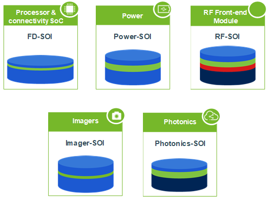
(Images courtesy Soitec. Note: darker bulk color indicates higher resistivity.)
We’ll start with FD-SOI since it’s most familiar, if not the oldest. Yes, some of this will be review to many of you. Never hurts!
The “FD” stands for fully depleted (in contrast to the partially-depleted versions). The deal here is that the top silicon layer is very thin – on the order of 10 nm. The benefit of such a thin layer is that it can be – surprise! – fully depleted for better electrostatic control.
The underlying BOX is also thin – around 20 nm. This gives FD-SOI an interesting potential capability (if exploited in its implementation). Just as a layer of oxide above the top silicon layer acts as a gate controlling a channel, so the thin BOX can act as a gate controlling that same channel. You can hit it from the front or the back.
This provides yet another knob for controlling the threshold voltage and, in particular, for ramping up performance or ramping down power dynamically.
Then there’s Power SOI – optimized for power electronics. So the silicon layer on top will be thicker – much thicker, meaning that the gate won’t be able to deplete the channel completely.
It has a thicker BOX layer to provide for a higher breakdown that isolates the high voltages being serviced on the die. In general, this is one of two flavors with dimensions specified in microns, not in nanometers.
RF-SOI adds a new ingredient. It turns out that, at high frequencies, electrons are generated and sent down into the bulk silicon. Recombination in the bulk is too slow, meaning that they stick around and accumulate. This messes with electrical characteristics, linearity, and the harmonics – not great when you’re processing radio-frequency signals.
So they add a so-called trap-rich layer. These traps act to quench the onslaught of errant electrons, keeping performance predictable and controlled.
Next is Imager SOI. It’s similar to RF-SOI in dimensions, but it doesn’t include the trap-rich layer since frequencies are much lower. It features sharp interfaces and extra-low contamination for sharp, high-resolution light detection.
Finally, we have Photonics SOI. Here, the top silicon layer is where the optical waveguides will be built, so it’s pretty thick – like Power SOI. The lasers themselves will be mounted atop the die, sending the signal into the waveguides. Thicknesses are again measured in microns – up to 1 for the top silicon and 1 to 3 for the oxide.
I’ll summarize here with a table.
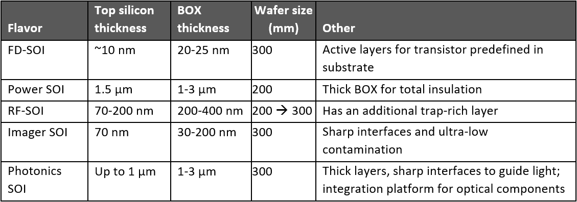
(Source: Soitec)
There are a couple of things that they say can be done with these technologies that give them an edge over FinFET technology.
- It’s easier to bring power down, particularly using FD-SOI’s back-gating capability. Soitec points to a Sony case where they lowered the power of a GPS receiver by 90-95%. This let them put the chip on a watch.
- Soitec says it’s easier to integrate embedded MRAM on FD-SOI than on FinFET technology.
- Soitec also credits SOI with greater immunity against soft errors (also true for MRAM).
Of course, the flavors given here might not be the best for absolutely everything. Soitec often meets with potential customers trying to start a project. In some cases, they decide to do some customization for the project – good because of flexibility, but you’re also limiting your sourcing options. In other cases, Soitec has to work with the customer to get the design changed to work with one of the flavors.
[Editor’s note: article updated to incorporate new data into the table and the significance of the darker color in the figures, as well as to reinforce that FinFET comparisons apply only to FD-SOI, not the other flavors.]
More info:


What do you think of these SOI variants?