


The old kid in town repeats, “Not so fast…”
When FinFETs came onto the scene, planar transistors were declared a thing of the past. Everyone fawned over the cool, creative new way to do transistors, riding a wave of public fascination with anything 3D. FD-SOI (fully-depleted silicon-on-insulator), a planar technology that addressed some of the older planar technology issues, struggled to remain relevant. You could practically hear them, all alone behind the crowd at a FinFET rally, exclaiming to anyone that would listen, “Wait, we’re still here! We’ve got some ideas! We’re still relevant!”
But FD-SOI was so… 2D. It didn’t fit the narrative that a cool new kid was in town and that cool old kids were no longer to be considered cool. And so the rally continued to shout the praises of FinFETs, while the FD-SOI guys got hoarse on the sidelines without attracting significant notice.
After the big party came the hangover. Oh yeah, there’s a cost to FinFETs. And, after a while, folks came trickling back to explore once again whether going 3D was inevitable. Things burbled along quietly until early this year, when GlobalFoundries announced their 22FDX offering, which took specific aim at applications that weren’t performance-at-all-costs. Good performance at lower power was the name of the game, without the cost and complexity of FinFETs.
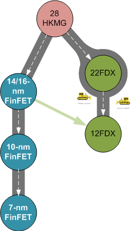
But it was one node. It was as if FD-SOI were getting a couple-year reprieve, holding on for one more last-gasp hurrah before taking its predestined place in the history books. While FinFET technology had its ongoing roadmap, FD-SOI seemed like something of a cul-de-sac – a place you could hang out comfortably for a while, but if you wanted to go anywhere new, you ultimately had to head back out to the FinFET arterial.
Well, slightly less than a year after announcing 22FDX, GlobalFoundries has come back with 12FDX: the next node after 22FDX. If two points make a line, then we have a roadmap, and they’ve now bulldozed through the end of the cul-de-sac to create an actual road that goes somewhere. OK, it goes only one more node, with no turnoff at the 14/16 neighborhood and stopping just short of 10 nm, but it feels like they’re picking strategic points that allow them to shelter The folks that are fleeing FinFETs without covering every node possible. The 12 node will be close enough to shelter 14/16 refugees.
GlobalFoundries is backing up this announcement with some follow-up progress on 22FDX. They’re saying that execution on the technology has progressed even beyond their promises. PDKs came out in Q2, as promised. EDA and IP (and the whole ecosystem thing) were promised for 2017; they’re now saying that will be Q1 2017, with tools from ANSYS, ATopTech, Mentor Graphics, Cadence, and Synopsys. IP is available today, and customers can already start prototyping.
As to some of the most critical parameters – performance/power and cost, they claim to be ahead of schedule. They’ve proven operation down to a 0.4-V supply, saving up to 70% on power vs. 28-nm HKMG (high-? metal gate), with leakage down to around 1 pA/µm of gate width. AC performance is ahead of where they expected it to be.
Meanwhile, defect density – a key determiner of cost – is nearing the level where the more mature 28-nm yields are for logic and SRAM. They’re trying to sell designers on the value of using the back bias as an additional knob – something that most designers aren’t used to. It can be used for non-run-time functions like tuning and trimming, low-granularity run-time functions like helping with power down leakage or adding a burst of power when needed, or high-granularity functionality by allowing applications to change the back bias, giving coders access in software.
Interestingly, however, while they tout greater than 500 MHz operation on an ARM A7 core running at 0.4 V, they’re touting the technology, in particular, for analog, based on its high-frequency characteristics – fT and fMAX, which you can see here outperforming 14/16-nm FinFETs.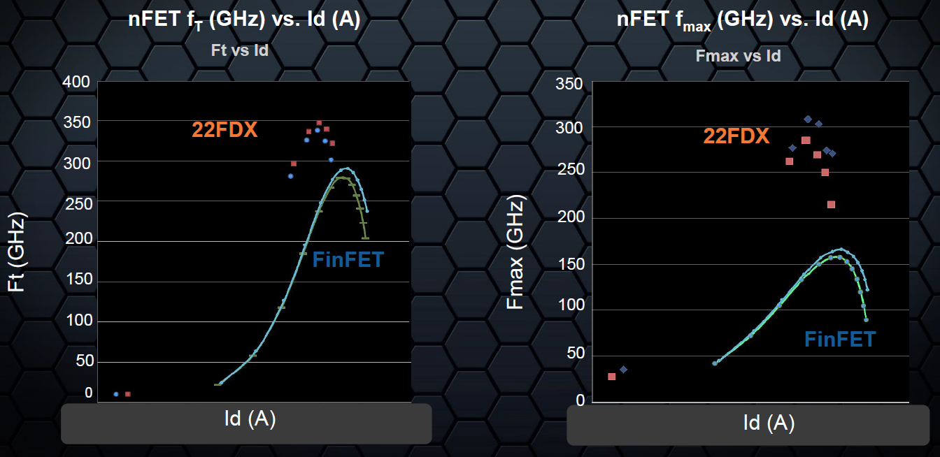
(Image courtesy GlobalFoundries)
So that’s where the already-announced 22FDX stands; the news is, of course, not 22FDX, but 12FDX. Scaling the technology hasn’t been obvious, but they’ve been able to leverage a lot of the work that IBM did to understand the fundamental scaling limits. One of their biggest remaining challenges is to work out the interconnect in a way that keeps the mask count – one of the biggest drivers of cost – reasonable.
That partly relates to multiple patterning for metal. Raising transistor density is great, but if you have to go through contortions to squeeze in the interconnect, you’ve still got a problem. That’s the balance they’re trying to strike, and it’s shaping up as a middle-of-line (MEOL) issue. Presumably some double-patterning will still be necessary, but they’re trying to keep it to a minimum. Their studies have convinced them that it’s doable, so, assuming that’s correct, all that’s left is the doing. The goal is to deliver “next-node” performance with 40% fewer masks than FinFETs require. (“a.u.” apparently stands for “arbitrary units,” meaning that the graphs are normalized.)
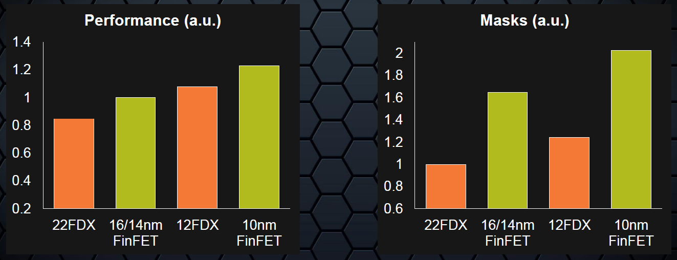
(Image courtesy GlobalFoundries)
They view the overall future of this thusly: designers that needed high performance back when 14/16-nm technology came available will continue on, but in 2019, when 12FDX is available, those same designers will be focused on 7-nm silicon, which will then be the leading edge. At that point, there will really be no reason for anyone else to use 14/16-nm FinFETs, since the same or better performance, with lower power, can be had at lower cost with FD-SOI.
One last reminder for the timing of all of this: 22FDX is gunning for customer designs in 2017; 12FDX is targeted two years later, in 2019. You will then be free to leave the cul-de-sac.
More info:
GlobalFoundries FDX technologies


Do you think FD-SOI will take a significant share of future designs instead of FinFET?
Interesting Article!!
Yes, FD-SOI will take a significant share of future designs mainly for IoT End nodes, where ULP with low voltage operation is the key requirement.