


Just over a month ago, GlobalFoundries (GF among friends) had their technology conference, and it would appear that they stored up all kinds of news to release at the same time. Some announcements were more significant than others; we’ll review what’s new here, with a focus on the bigger issues and a passing nod to the others.
I Could Use a Shrink
Some of you out there may remember a quaint notion from the ancient semiconductor past: the shrink. In fact, you may have a particularly fond place in your heart for the best of the shrinks: the optical shrink. Imagine… a new process node with no design work. Just put the mask design in the equivalent of a copier with reduction capability, dial up the shrink, and boom! New process node. Time for a beer.
Yeah, that hasn’t really happened in a while. (Including beer during work.) These days, each process node means more or less starting a new design. Too much stuff changes between nodes.
So you can imagine that my interest was piqued when GF announced that they were providing a 12-nm FinFET technology node that is a shrink of their 14-nm platform. Not an optical shrink; work is required to move a design from 14 nm to 12 nm. But the idea is that you don’t have to start from scratch; logic area should shrink easily.
They call it their 12LP process, based on 14LP. But they compare the specs to industry-“standard” 16-nm processes, with up to 15% denser circuits and 10% less power than 16 nm. Risk starts should be available early next year.
This isn’t a replacement, of course, for the more aggressive nodes in the 10- and 7-nm range; they’re working that one independently. 7 nm will be their first node using extreme-UV (EUV) lithography, and yeah, sorry, there’s no such thing as taking all the “colored” multi-patterning masks for one layer and combining them into a single, shrunk, uncolored EUV mask. Not even close. It’s gonna be real work, in the tradition of modern process node changes.
They’re projecting a 40% increase in performance and a 60% decrease in power at the 7-nm node as compared to 14LP. They expect this to yield ARM A72 performance of over 3.5 GHz.
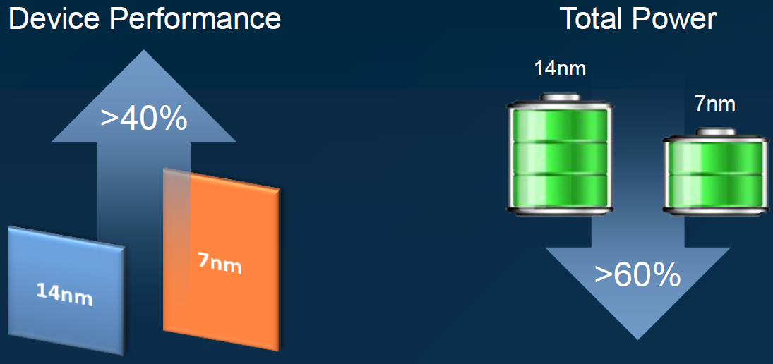
(Image courtesy GlobalFoundries)
Moving to 5! Gee!
Next we move to their RF offering. They largely motivate it by the move to the next generation of cellular wireless technology, 5G, which we looked at late last year. Turns out there are two frequency regimes in 5G that they say will yield over 10,000 band combinations. The first is referred to as sub-6, since the frequencies in that range are all below 6 GHz. It’s reasonably accessible in the nearish term. The other regime is in the mmWave region.
The mmWave bands haven’t been completely sorted yet. Generically, we’re talking the range between 30 and 300 GHz, although not all of that spectrum is available for wireless use. There are numerous complexities that 5G brings in an attempt to wrest as much data throughput as possible from these bands.
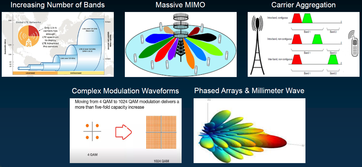 (Click to enlarge; image courtesy GlobalFoundries)
Their announcement for this challenge was their 8SW process, based on an RF-SOI technology. Yeah, the naming of this node is distinctly different from that of their other non-RF nodes. It’s a legacy effect from a process originating at IBM. They describe it as a 130-nm process that permits 55-nm features. They’re claiming 70% better performance than the prior 130RFSOI node, with 50% smaller dice.
For enabling mmWave designs, they point in two different process directions. For designs where the focus is the front-end module (FEM), they point to their 45RFSOI node. If integration is more important than all-out FEM performance, then they indicate their 22FDX node – the FD-SOI process we looked at back when announced. But this is a newly-announced mmWave variant.
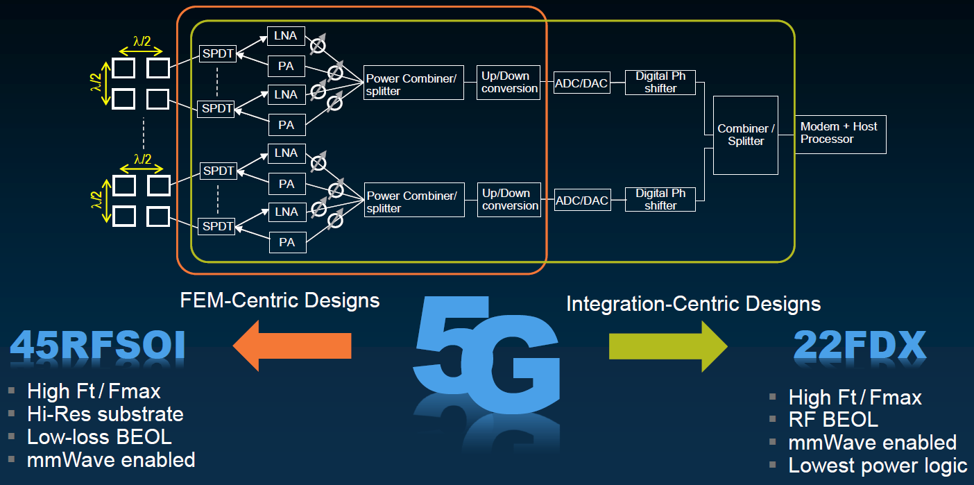 (Click to enlarge; image courtesy GlobalFoundries)
But Wait! There’s More!
Elsewhere in their big-ol’ pile o’ announcements were the following:
- They’ve now made embedded MRAM (eMRAM) available on their 22FDX process node. We’ve looked at MRAM a few times before, and, in the most recent piece, we mentioned this integration from Everspin. At that time, it was a work in process; that work is now complete.
- They announced an updated SOI wafer supply agreement with Soitec. We recently looked at the various SOI flavors available courtesy of Soitec, but, of course, each foundry commercializes their own flavors. That said, Soitec is the primary source of SOI wafers. Having a single-source is sometimes unavoidable, but it is generally to be avoided where possible (at least by customers trying to dodge vendor lock-in). So GF is trying to enable additional sources in the future in order to help to put downward pressure on wafer prices.
- They announced their 14HP (high performance) process for use by IBM in their processors that feature in mainframe computers. Yeah, no IoT here! What’s unusual about this process is that it’s based on an FD-SOI platform, but it uses FinFETs. It’s interesting that they make this announcement largely for the benefit of a single (albeit influential) customer.
- Finally, they announced that Synopsys’s design platform was certified for 22FDX. Announcements like this are pretty routine for new process nodes for all the EDA majors and foundry majors. This happened to coincide with all the other non-EDA news. You’d think that 22FDX would be just another process node to support, but there’s one critical 22FDX (and 12FDX) capability that is unique to this family: the ability to back-bias transistors for tailored – and even real-time adjustment of – performance vs. power. That’s a new knob that can be turned, and it was one of the challenges leveled at the technology by the competition. But the feature is supported in an automated fashion for GF-certified flows; EDA support is summarized below.
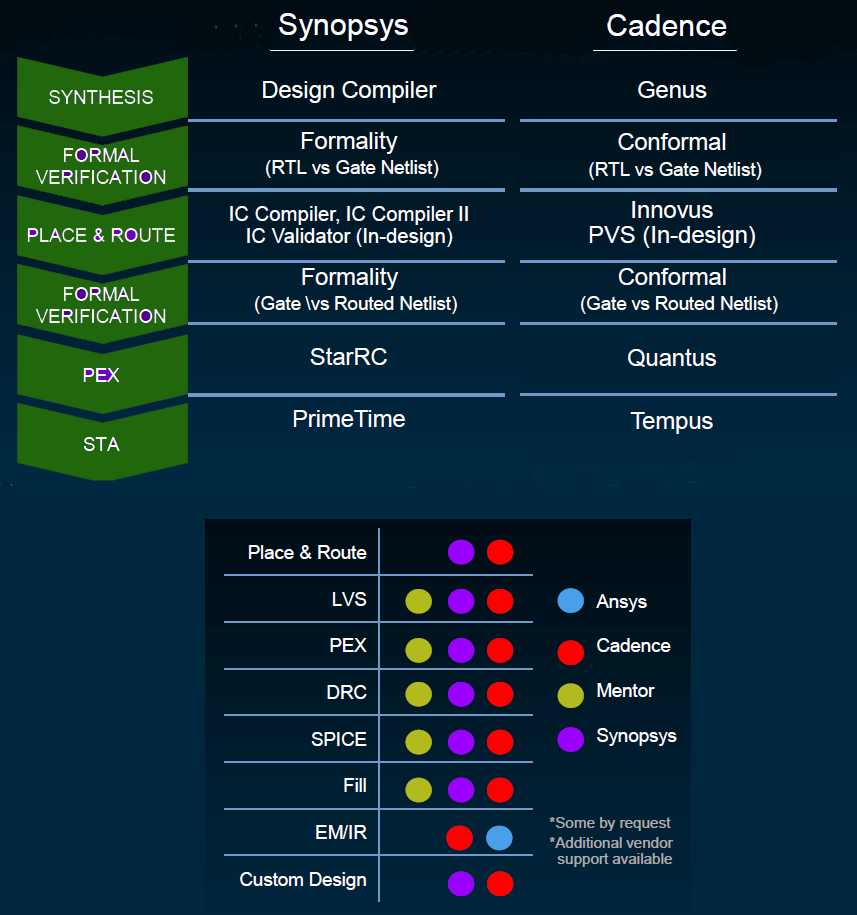
(Based on an image courtesy GlobalFoundries)
Whither From Here?
CTO Dr. Gary Patton also presented a look at where things are going on the performance side. After all, FinFETs are all the rage today – and yet, they’ll run out of steam at some point. Next up, for even better electrostatic control, would be nano-wires (also referred to as “gate all around, or GAA”) or nano-sheets. Nano-wires may also go vertically at some point – turning into something that I like to call a “PinFET.” The dates on the image below relate to research breakthroughs in collaboration with the IBM Alliance.
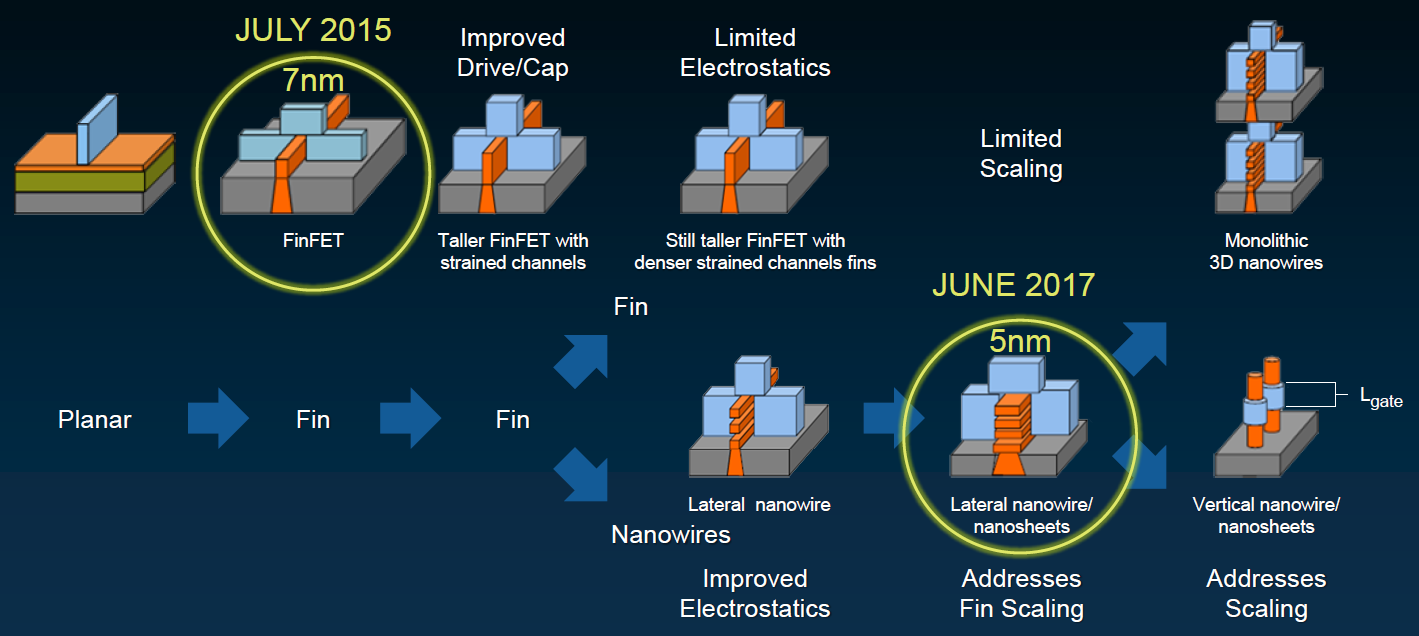 (Click to enlarge; image courtesy GlobalFoundries)
And that rounds out the announcements; you can learn more at the various links below.
More info:


What do you think of GlobalFoundries’ announcements and roadmap?