featured chalk talk
Time to first prototype shouldn’t be so hard!
In this episode of Chalk Talk, Romain Petit from Siemens and Amelia Dalton examine the challenges of FPGA-based prototyping and how the automatic partitioning, automatic cabling, runtime and debug infrastructure and more of the Siemens VPS platform can make your next FPGA-based prototype project easier than ever before.
featured chalk talk
Veloce proFPGA CS First to Market with VP1902
In this episode of Chalk Talk, Oz Levia from Siemens and Amelia Dalton explore the trends pushing a need for hardware-assisted verification, how modularity can speed up system design, and the benefits that the Veloce proFPGA CS platform can bring to your next design.
featured chalk talk
Driving innovation in 3D IC Design: Siemens Calibre MultiPhysics Work Flow
In this episode of Chalk Talk, John Ferguson from Siemens and Amelia Dalton explore how we can drive 3D IC innovation with Siemens Calibre MultiPhysics Work Flow. They also investigate the implications of thermal issues on 3D IC design, the benefits of multiphysics simulations from the concept stage throughout the design cycle, and the steps included in the Siemens fully automated MultiPhysics Work Flow.
featured chalk talk
Insight Analyzer: Design-Driven Reliability Verification
In this episode of Chalk Talk, Matthew Hogan from Siemens and Amelia Dalton explore how Siemens Insight Analyzer can help designers identify and address design-specific potential circuit reliability failure areas. They also examine how Insight Analyzer redefines comprehensive circuit verification and can be a compelling addition to “shift-left” strategy.
featured chalk talk
Accelerating Time to Fault Campaign Success with Siemens EDA
In this episode of Chalk Talk, Ann Keffer and Robert Serphillips from Siemens and Amelia Dalton explore how the Siemens EDA functional safety platform can guide your team through the complete ISO 26262 lifecycle. They also examine the benefits that the Veloce Fault App brings to automotive IC designs and how you can take advantage of the full suite of functional tools from Siemens EDA for your next automotive IC design.
featured chalk talk
SIRIUS Modular System
In this episode of Chalk Talk, Sarah Alqaysi from Siemens and Amelia Dalton investigate the Siemens SIRIUS Modular System. They explore how this system of motor starters, contactors, overload relays, and load feeders can help switch, control and protect the motors in your next design.
featured chalk talk
FPGA-based Prototyping with the Latest High-Capacity FPGA Enables New Use Modes
FPGA-based prototyping is an essential tool for any SoC and digital chip design and verification. In this episode of Chalk Talk, Juergen Jaeger from Siemens and Amelia Dalton explore the multitude of benefits of the Veloce proFPGA CS platform from Siemens. They also investigate the debug capabilities, software prototyping and scalable hardware of this solution, and how you can use the Veloce proFPGA CS solution for your next design.
featured chalk talk
Calibre DesignEnhancer: Layout Modifications that Improve your Design
In this episode of Chalk Talk, Jeff Wilson from Siemens and Amelia Dalton investigate the variety of benefits that the Calibre DesignEnhancer brings to IC design and how this tool suite can be used to find and fix critical design stage issues. They also explore how the Calibre DesignEnhancer can Identify and resolve issues early in design flow with sign-off quality solutions and how you can utilize Calibre DesignEnhancer for your next design.
featured chalk talk
Shift Left Block/Chip Design with Calibre
In this episode of Chalk Talk, Amelia Dalton and David Abercrombie from Siemens EDA explore the multitude of benefits that shifting left with Calibre can bring to chip and block design. They investigate how Calibre can impact DRC verification, early design error debug, and optimize the configuration and management of multiple jobs for run time improvement.
featured chalk talk
Shift Left with Calibre
In this episode of Chalk Talk, Amelia Dalton and David Abercrombie from Siemens investigate the details of Calibre’s shift-left strategy. They take a closer look at how the tools and techniques in this design tool suite can help reduce signoff iterations and time to tapeout while also increasing design quality.
featured chalk talk
Solutions for Heterogeneous Multicore
Multicore processing is more popular than ever before but how do we take advantage of this new kind of processing? In this episode of Chalk Talk, Jeff Hancock from Siemens and Amelia Dalton investigate the challenges inherent in multicore processing, the benefits of hypervisors and multicore frameworks, and what you need to consider when choosing your next multicore processing solution.
featured chalk talk
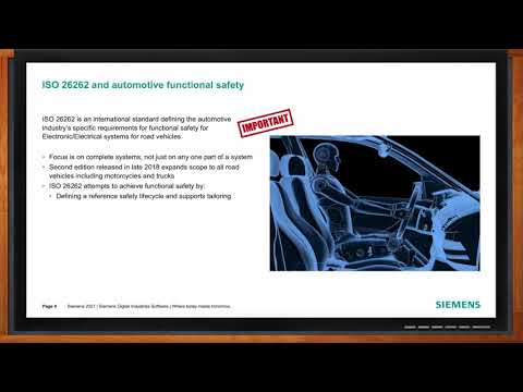
Software and Automotive Safety
In the realm of automotive designs, safety must reign above all else. But the question remains: How can we innovate within the constraints of today’s safety standards? In this episode of Chalk Talk, Amelia Dalton chats with Rob Bates from Siemens about the role ISO 26262 plays when it comes to COTS and open source software, what certified software components are all about, and how heterogeneous multiprocessing can be helpful in your next automotive design.
featured chalk talk
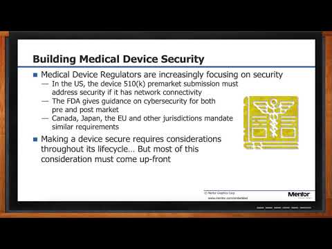
Medical Device Security
In the new era of connected medical devices, securing embedded systems has become more important than ever. But, there is a lot medical device designers can borrow from current best-practices for embedded security in general. In this episode of Chalk Talk, Amelia Dalton chats with Robert Bates from Mentor about strategies and challenges for securing modern medical devices and systems.
Keeping Your Linux Device Secure
Embedded security is an ongoing process, not a one-time effort. Even after your design is shipped, security vulnerabilities are certain to be discovered - even in things like the operating system. In this episode of Chalk Talk, Amelia Dalton chats with Kathy Tufto from Mentor - a Siemens business, about how to make a plan to keep your Linux-based embedded design secure, and how to respond quickly when new vulnerabilities are discovered.