

It was the coolest transistor development in many a year. Rather than continually squishing transistor parts closer and closer together, we flipped it to vertical and celebrated the arrival of the FinFET.
Which was great: it gave us a way to keep increasing performance in many of the applications where the value lies in the speed of the circuit. But after the initial party was over and we started picking up the pointy party hats and nursing the hangovers with massive doses of ibuprofen, we started looking at the bill. FinFET is nice, but it’s also expensive. And, while we’re throwing stones, it’s also not so great for analog and RF designers based on the quantized nature of the gate. You can’t increase channel dimensions by 1.5 times; it’s either 1 or 2.
FinFET has been billed as the future of silicon, and Intel jumped on it, meaning everyone else had to as well. But that pounding morning-after headache is pretty strong, and there are folks wishing they had an alternative to FinFET.
We’ve talked in the past about the competition between FinFET and the other technology waving its hands to get noticed, FD-SOI (fully-depleted silicon-on-insulator). Problem is, according to GlobalFoundries, the last generation of FD-SOI just didn’t have the performance to compete even in applications not requiring full FinFET speeds.
Also, back then, it was a FinFET-vs-FD-SOI thing. And once Intel committed to FinFETs, the feeling was more or less that FD-SOI had lost out. But now that folks are sitting back and considering that FinFETs might not be the solution to all problems, the possibility of co-existence raises its head.
GlobalFoundries has taken this seriously enough to develop a 22-nm FD-SOI process for use when FinFETs aren’t needed. Called 22FDX, they announced it last summer, and I got a chance to talk to them about it during last month’s IEDM conference. They see it as the first in a number of steps that can take them as far as the 10nm node. It won’t have the full-throttle performance of FinFET, but, on a bursty basis, it can compete in some applications that require speed – as well as those that don’t. And it has some specific EDA implications that we’ll need to explore.
What’s different about this FD-SOI is that it can drive VT down as low as they think is feasible, while allowing custom – and even dynamic – back-biasing to tune the VT and get performance or reduce power where needed. Based on dynamic and leakage energy dissipated as a function of VT, they have determined 0.4 V (roughly) as a bottom VDD target.
Note that this is intended for above-threshold designs. They see a place for near- and sub-threshold designs in certain areas, but they say that such circuits will suffer in performance as compared to super-threshold circuits. So, even though the VT is low, the transistors are intended for above-VT usage.
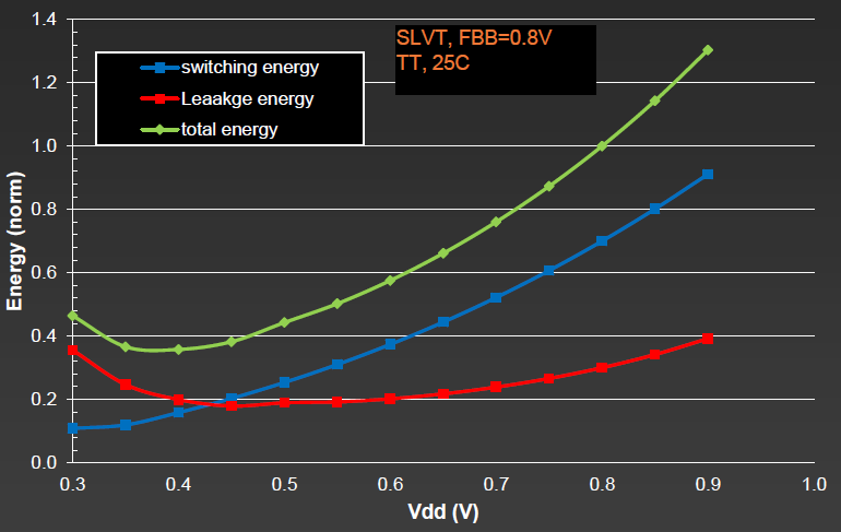
Image courtesy GlobalFoundries
To be clear, this isn’t an indictment by GlobalFoundries of FinFETs in general; they make FinFETs, and if a customer wants that, great. But this provides an alternative path below 28 nm – the first such alternative in the market, they claim.
One of the big contributors to FinFET cost is multiple patterning – double and even quadruple. They haven’t been able to completely eliminate it, but they have limited it to the first and second metal layers. No multiple patterning is needed for the transistor or the higher metal layers (or the vias between them).
As far as performance is concerned, FinFET-performance-level operation isn’t as energy efficient as it would be with a FinFET. This is why, for full-on sustained performance, a FinFET is the better choice. But if you need that performance only on an occasional, bursty basis, then the overall FD-SOI savings can give you that speed at less cost and potentially lower energy overall.
Compared to their 28-nm 28SLP-HKMG process, the performance of a Cortex A7 processor yielded 92% less power if VDD was taken down to 0.4 V, or 47% less power at the same frequency, or 50% faster with 18% less power. Notably, they were able to achieve 1.2-GHz performance – equivalent to FinFET speed. As you can see, the FinFET uses less power overall for a given frequency, which is expected; it’s just so danged expensive.
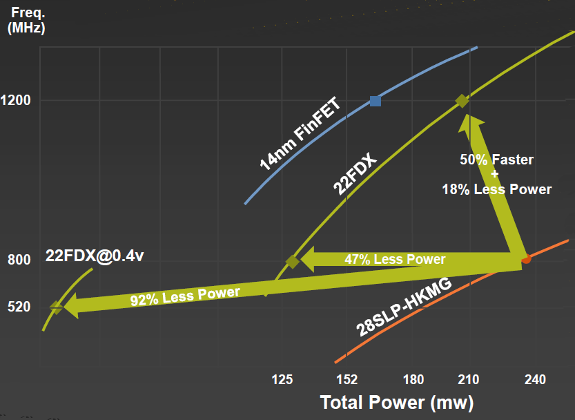
Image courtesy GlobalFoundries
They’ve also completed a Cortex A17 quad-core demonstration chip, using 5 power domains (one for each CPU, plus one for the non-CPU stuff) and 5 biasing pairs (n-well and p-well; one pair for the standard cells, two for the L1 cache, and two for the L2 cache).
GlobalFoundries certainly considers 22FDX a better choice for RF and analog, and one of the benefits of going in that direction is that it lets you combine RF and analog with digital on a single chip more easily than can be done with FinFET. So integration benefits may also tilt a process decision towards FD-SOI.
Design and tool considerations
It’s typical for a given process node to have several variations on the transistor to optimize for speed or energy or some other parameter. What’s unusual with 22FDX is that they have a veritable constellation of options – which is one of the areas that may require more EDA attention. Because the choice of transistor really should be made by the tools based on the performance and energy constraints of the design.
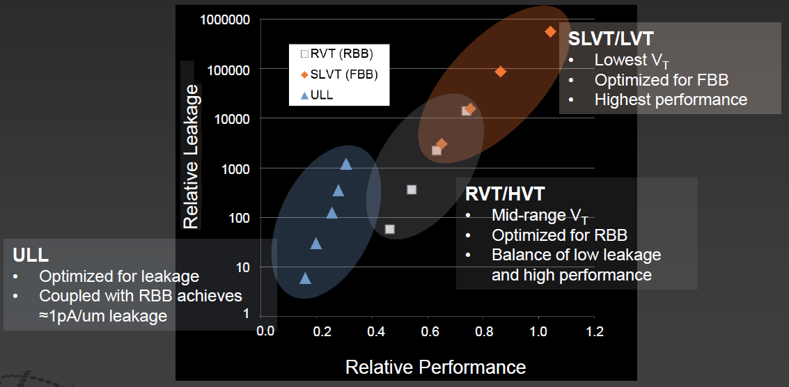
Image courtesy GlobalFoundries
But things get more bizarre with the back-bias options – both positive and negative. Some of the simpler options are engaged by picking the appropriate transistor. The tools would need not only to pick the best transistor option, but also to instantiate the back-bias circuitry that will deliver the VT that will yield the desired speed/power point.
Given the need for different transistors in different places, you can create blocks, each of which has a different back bias. If multiple blocks need the same bias voltage, then a single bias generator output can be shared between those blocks. So it’s not one generator per block, but rather one generator per bias level. This lets you amortize the extra area for the generator over all the blocks that use it.
But then there’s the flashy aspect: the ability to change the back bias on the fly during operation. This could be particularly useful for highly bursty blocks that are asleep for much of the time. While sleeping, the transistors could be optimized to keep leakage low; when awake, software could direct the chip to change the bias level for higher performance during the on cycle, reverting to the original bias level when the burst is complete and the block is going back to sleep.
This adjustable nature of the bias can also be used to help trim in analog blocks, potentially saving a mask turn or even making chip-by-chip adjustments during test (assuming some NVM cells to store the new trim level).
But some of the automation that you might dream up hasn’t made its way into the EDA tools, as far as I can tell. From a digital logic standpoint, at a high level, it would seem that the overall circuit has specific power and speed constraints that will determine, among other things, which transistors to use, which determines which VT to use, which will then determine the necessary bias voltage. In other words, in theory, it would seem that you could abstract much of this away from the digital designer – at least when it comes to static bias levels.
But it’s a bit messy. The logic path optimization happens through logic synthesis, but the bias level is treated more like power, and it’s driven by the UPF file and power synthesis. Specifically with Mentor Graphics, floorplanning will establish which blocks need which bias signals and they will automatically place and route those signals correctly. But deciding which bias levels are needed and instantiating the bias voltage generators must be done manually; there’s no synthesis step that works back from speed/power constraints to automatic instantiation of bias generator IP.
The bias generators will ultimately be available from GlobalFoundries’ IP library, so digital designers won’t have to manually design the generators; they’ll need to parameterize the generators from the library. This is particularly true for dynamic bias generation; there will also be an IP block for that, converting a digital signal into the selection of appropriate bias levels, but it must be manually put in place.
And, of course, GlobalFoundries has a boatload of IP planned so that all of the sorts of circuits available for FinFETs are also available for FD-SOI, including numerous NVM options.
I also checked in with Synopsys and Cadence. Synopsys basically had no comment, and Cadence said the information was proprietary. I’m assuming that, in the latter case, it will be public eventually so that designers know what they need to do. All three of the big guys plus, at the very least, ATopTech announced 22FDX support in November.
So, all in all, we have what promises to be a less expensive alternative to FinFETs, with possible scalability to 10 nm. It can achieve FinFET performance, although less efficiently. If such performance is desired on a bursty basis, this can work. Performance on a sustained basis still calls for FinFETs. There’s some more design work needed to establish the bias levels; it seems like that will add a nominal amount of work once all the required IP blocks are in place. And it feels to me that, if there’s demand for this process, that more automation could be put into place.
[Editor’s note: article was changed to correct reference to 0.4-V VT. VT should have been VDD.]
More info:


Do you see FD-SOI as a useful partner to FinFET technology for non-performance-intensive designs?
FD-SOI is better than FinFET for a couple of reasons, one being you can switch between high-power/performance to low-power/performance just by changing the back-biasing, whereas FinFETs would need to use DVFS, i.e. if you just use clock gating in a design you can switch the BB mode to match clocks being off/on and not bother with LDOs etc.
FD-SOI also has lower variability, and much better analog characteristics than FinFET, and all together it’s probably the best process for IoT and other power sensitive mixed signal applications.
The “fly in the ointment” for FD-SOI is (as mentioned) that the standard (RTL) digital design flow doesn’t understand power at all well, i.e. there’s no support for DVFS, let alone back-biasing in (System)Verilog, and that pushes you into using much slower “fast” SPICE for verification – Chris Rowen talked about that at a recent Cadence event for non-FD-SOI processors.
Having said that there is support in the last Verilog-AMS standard for making analog/digital simulation boundaries Vdd/Vss aware, and that mechanism also works for back-biasing. I added the support to one simulator myself (although it’s unlikely it’s in the documentation). There are also ways to break out of standard simulation in the latest SystemVerilog to add the extra functionality needed. Both those approaches would be close to the speed of the standard functional verification.
If anyone needs help with that let me know
http://www.linkedin.com/in/kevcameron
……