


Seems like we’re never happy with our memories. No matter how hard we work, how clever we get, there’s always something left to be desired.
Which is why, of course, we have complicated system memory architectures mixing different memory types with different characteristics so that we can, as a whole, compensate for the deficiencies. Your typical computing platform contains three radically different types of memory: static, dynamic, and non-volatile (NVM) – and yet it’s still not satisfying.
Today we look at a few more new announcements. One is of a full memory, available today, targeting small to medium embedded devices in the IoT or wearables realm. The others deal with future technology – frankly, one that’s been perennially a future technology. Will it be different this time?
Adesto Fideles
We start with non-volatile memory that’s more or less familiar, but with some catchy new features. It’s targeted at execute-in-place (XiP) applications for smallish devices – this is the IoT/wearables thing.
The fit is aimed at low-end, inexpensive microcontrollers – ones that aren’t going to have on-board embedded flash memory. That means they need off-chip non-volatile code storage. NOR flash used to serve that purpose in general, although it has started to lag since it can’t be made economically large enough to handle big programs. For those big programs, NAND flash is used – but you can’t execute directly out of NAND flash, so it has to be preloaded (or “shadowed”) into on-chip memory for execution.
But if you’re still in that smallish range (up to 32 Mbit), Adesto has announced a new NOR-based flash memory, called EcoXiP, with some enhancements that help with the whole XiP thing. And, really, their new features don’t affect the memory technology itself; they affect how you get to the memory – and how quickly.
NOR flash has moved from parallel to serial interfaces, using SPI as the basis – typically up to a quad version. Adesto has implemented an octal version (OPI) in order to get data more quickly without increasing the clock speed.
They then added a feature to the protocol to make prefetching code much more efficient. Ordinarily, you fetch a line at a time, and, if you want multiple lines, you issue successive commands – one for each line. This uses a lot of SPI time for the repeated commands – it’s like having a really small limit on a DMA, forcing you to break up a big DMA operation into a bunch of small independent ones.
They modified this capability in a couple of ways. First, if there’s a particular known byte that’s needed, the readout can start there (rather than having to start at the beginning of the row and throwing away data until you get to the byte you care about).
Next, when it gets to the end of the line, instead of wrapping around to the beginning of the same row – traditional behavior – it automatically increments down to the next row. So you can read out multiple successive rows with just a single command. They say that this feature, which they call “command fusing,” effectively speeds up the CPU by 41% without increasing the clock speed.
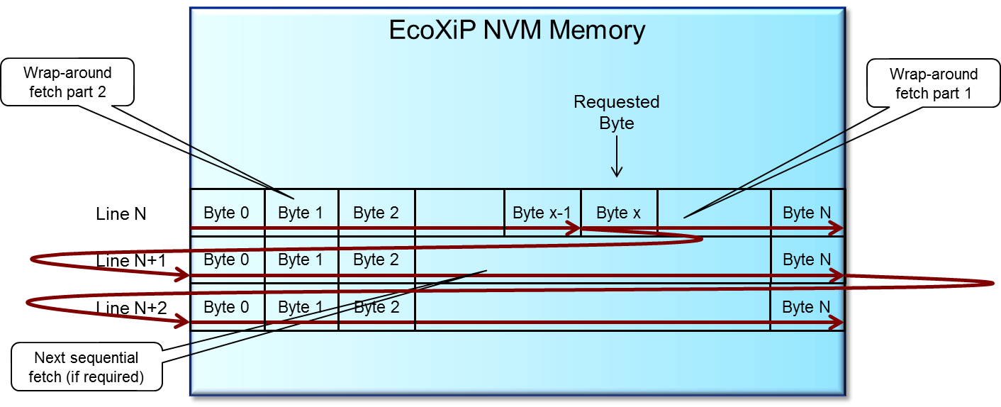
(Image courtesy Adesto)
Another improvement they’ve made affects updating. Apparently, older parallel-interface NOR flash devices allowed simultaneous reading and writing, but that disappeared with the transition to serial interfaces. Adesto has brought it back, allowing a read in one bank while writing to another bank. This allows execution to continue even as the code is being updated.
Finally, they’ve added some features to save power:
- The performance-enhancing features mean they can operate with a slower clock.
- They’re providing programmable I/O drive, so you can drive hard if you have a long trace, or drive softly if not.
- They have an auto-power-down mode. Traditionally, if using the memory infrequently, you can shut the memory down to save power; Adesto has provided three levels of power-down mode. But CPUs also like to sleep when not being used. When you write to the memory, which takes time, the CPU normally has to stay awake so that, after the write is done, it can turn off the memory. Adesto has added a write-and-then-shut-down feature so that the CPU can launch the write and go immediately to sleep; the memory will shut itself off after completing the write operation.
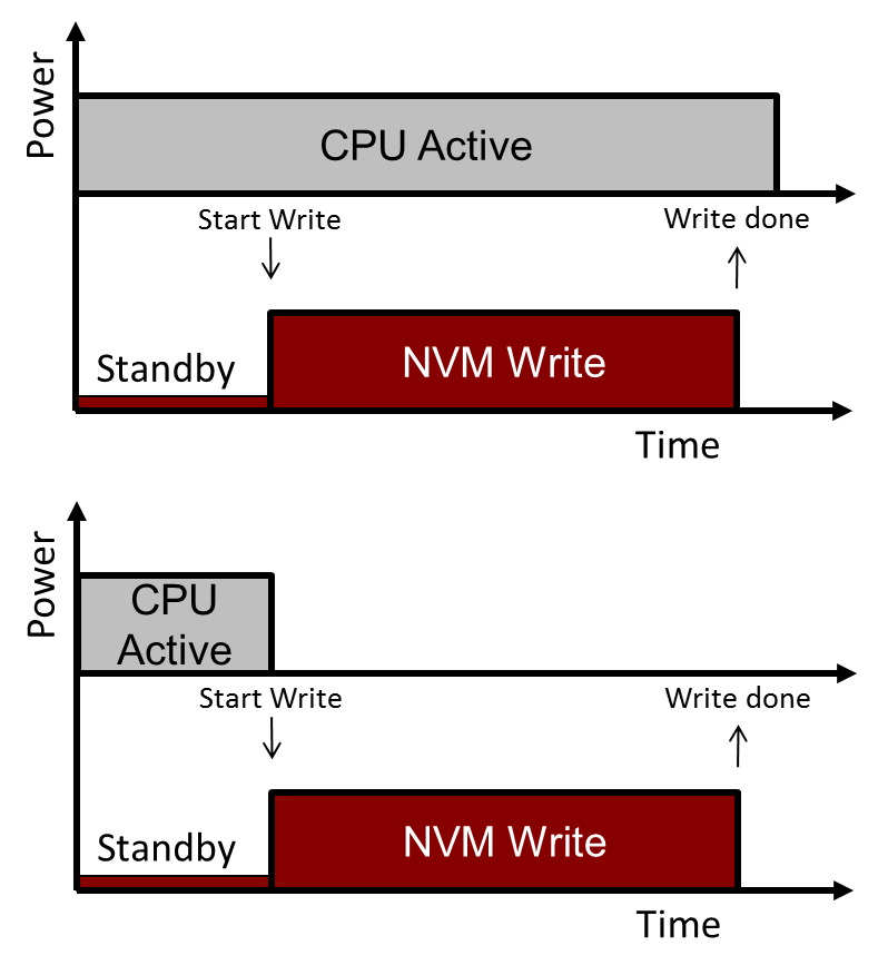
(Image courtesy Adesto)
Mmmmm… RAM
Next we move to a technology we haven’t discussed for a while: MRAM. And we have noise from two players here.
First, the more established player: Everspin (which recently completed an IPO). GlobalFoundries is partnering with them, adding MRAM to their 22FDX FD-SOI platform (and, in the future, to FinFET and the recently announced – and covered – 12FDX platform). Of course, GlobalFoundries provides flash memory technology as well, so they’re positioning MRAM as an option without necessarily disparaging the other option(s).
They largely show it replacing SRAM – in fact they’re working on a new memory architecture that will leverage the benefits of MRAM, which can be packed eight times more densely than SRAM on an SoC. MRAM also excels in read/write speed as compared to NVM. And, in keeping with our theme, it’s also well suited to XiP applications – with IoT as an application space in sight.
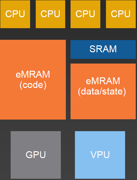
(Image courtesy GlobalFoundries)
MRAM has gone through a number of iterations. When we first looked at it, the so-called “free” layer – the one that you can flip magnetically – was magnetized by a current in a loop around the cell. This took a lot of power and, critically, got in the way of scaling. As device size dropped, they figured out how to do “spin-torque transfer,” or STT.
The idea here is that you take a current and filter it so that it consists primarily of electrons all spinning in the same direction. You then run current that through the magnetic layer in the expectation that all those polarized electrons will induce the electrons in the magnetic layer to polarize in the same direction – effectively transferring the torque from the incoming electrons to the local ones.
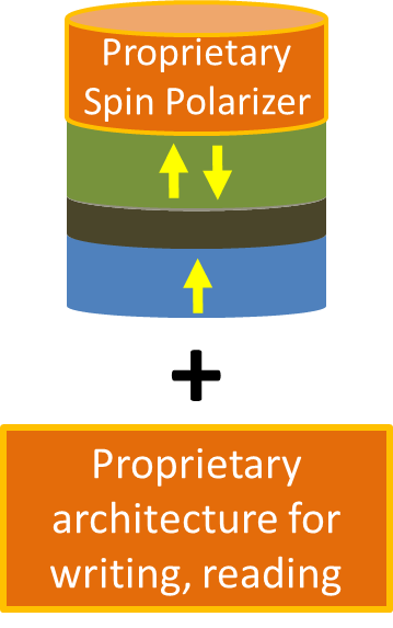
The green layer is the free layer; the blue layer is the pinned layer; and the gray layer is the tunneling layer that separates them.
(Image courtesy Spin Transfer Technologies)
The first generation of STT (which is the second generation of MRAM) created an in-plane magnetic field; the latest generation creates a perpendicular field. (Which, if you’re counting, makes this the third overall MRAM generation.)
There is also a newly unveiled company called STT (which stands for Spin Transfer Technologies… yes, this might get confusing as to whether we’re talking the company or the generic technology – I noticed they refer to the technology as ST-MRAM rather than STT). As they describe it, there’s this triangle of characteristics related in a “pick any two” manner: speed, power, and endurance. You can’t optimize all three at the same time.
They’re newer at this; while Everspin is shipping product, STT (the company) is still developing their technology. They use their own research fab in Silicon Valley, which allows them much faster turn-around on the experimental wafers needed to dial in the process. Using a foundry can result in a 1-1/2- to 2-month delay just to get the magnetic layers laid down. And it takes about 50-100 “turns” – runs through the process – to finalize the process for production-quality yields.
By using their own fab, they say they can turn the back-end (the magnetics reside between the top two layers of metal) in 10-12 days – 6 days for a hot lot. This means they can burn through all those turns much more quickly. The goal is to get the process to the stage that it can be transferred to a commercial foundry without it becoming a new development process in the foundry.
To be sure, the stack includes about 20 different elements – and fab managers get queasy around new materials. But there’s nothing here, including equipment requirements, that hasn’t already been used for disk-drive heads (which use individual MRAM cells as sensors). The back end is typically walled off from the front end transistor processing anyway, so they say that there’s really nothing here that should cause any headaches.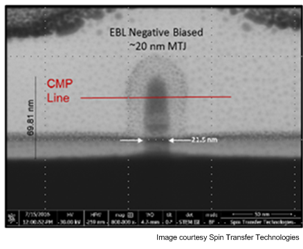
One of the enhancements STT is touting has to do with that infernal feature triangle. If you can’t optimize them all at the same time, then you have to pick winners and losers. But what if you want different winners and losers, depending on what you’re doing in a system? The knobs that affect where an array will sit in that triangle are voltage and pulse time (which themselves have an unholy triangle with write error rate) – and they plan to expose those in a manner that lets an application re-optimize dynamically – possibly even using software. If you suddenly need more speed, then crank it and go – spinning it back down when done.
In general, they’re also touting faster read and write speeds – not just faster than NVM, but also faster than existing MRAM. Everspin MRAM has access times in the “10s of ns”; STT is expecting write times under 10 ns and read times of “a few” ns.
All of that said, STT has more to prove. The thermally-assisted switching MRAM we looked at with Crocus years ago has yet to play out, for instance (the last we heard from them was using their technology for sensors). STT needs to get up quickly while keeping potential customers confident that they’ll deliver where others have stumbled.
Both GlobalFoundries and STT plan to license their MRAM for use in SoCs. GlobalFoundries is not really interested in making dedicated memory chips, since that typically takes a dedicated high-volume fab. STT is more open to it, although very cautiously.
As to timing, GlobalFoundries is expecting to sample customers in 2017; full production is in 2018. STT, meanwhile is on… basically the same schedule, with samples next year and products in 2018.
More info:


What do you think of Adesto’s XiP NOR flash and the MRAMs from GlobalFoundries/Everspin and STT?