


Are you involved in developing SoCs? Are you banging your head against the wall, desperately trying to determine why you aren’t obtaining the performance promised by the providers of your processor, interconnect, and DDR memory controller IPs? Do I have good news for you? (Spoiler alert. The answer to the last question is a resounding “Yes!”)
In many ways I envy the young engineers who are coming up today because they have such awesome technologies to play with. On the hardware side, they can create sophisticated SoCs containing billions of transistors implemented in eye-wateringly small semiconductor process nodes. On the software side, they can create cunning applications that employ artificial intelligence (AI) and machine learning (ML) in all their multifarious manifestations.
All of this is enhanced by sensors we could only dream of back in the day. For example, in addition to high-definition color cameras, today’s embedded systems developers have access to highly-sensitive microphones (see Acoustic Detection of Drones and We Already Have Cars That Can See, How About Cars That Can Hear?) and 4D radar (see Reimagining Radar in the Form of High-Resolution 4D Sensing Systems) and FMCW lidar (see FMCW LiDAR Can Perceive and Identify Objects More Than a Kilometer Away) and new night vision sensors (see Within Five Years, All New Cars Will Be Able to See at Night!) and… the list goes on…
I’m also thinking of teeny-tiny sensors like the BNO055 from Bosch Sensortec. This little beauty provides microelectromechanical systems (MEMS) realizations of a 3-axis accelerometer, a 3-axis gyroscope, and a 3-axis magnetometer, coupled with a 32-bit Arm Cortex-M0+ to perform on-chip sensor fusion, all presented in a single 3.8mm x 5.2mm x 1.13mm package. This inertial measurement unit (IMU) device can be purchased standalone or on a breakout board (BOB), such as the 9-DOF (degrees of freedom) absolute orientation IMU BOB from Adafruit. You can use it in all sorts of applications, including hobby projects, such as when I added one to my 12×12 array of ping pong balls, each of which contains a tricolor LED, for example.
The fact that we can afford to use this sort of sensor in an humble hobby project blows my mind. When I was a lad, sensors like an accurate 3-axis gyroscope were the size of small oil drums and cost hundreds of thousands of dollars, so you typically found them only in mission-critical systems like B-52 Stratofortress strategic bombers, just the saying of which immediately makes two movies spring into (what I laughingly refer to as) my mind: Dr. Strangelove and Dark Star.
However, there is a fly in the soup, an elephant in the room, and a goat guarding the cabbage field (I never metaphor I didn’t like). The issue at hand is getting the maximum amount of performance out of one’s SoC-based system. This is non-trivial, leading many SoC developers to leave unused performance sitting on the table.
Things used to be much easier in the old days when an SoC contained a single processor connected to a handful of other functions by a traditional bi-directional bus. In addition to any internal RAM and ROM memory, the SoC communicated directly with external memory components, and the performance of the entire device was essentially 100% deterministic.
Those days have long gone. Each of the (potentially) hundreds of intellectual property (IP) blocks on today’s SoCs can be larger than an entire device from just a few years ago. These IPs are no longer connected by a simple bi-directional bus. Instead, the designers may employ one or more chip-spanning network-on-chip (NoC) interconnect IPs in which data is packetized and serialized and large numbers of packets may be “in-flight” at the same time.
Today’s SoCs rarely have a single processor core (their designers would scoff at the idea). Instead, they have “processor clusters.” Consider a cluster of four processors, for example. One common configuration is for each processor to have its own Level 1 (L1) cache, for pairs of processors to share an L2 cache, and for all four processors to share an L3 cache. Cache coherency within the cluster will be maintained using in-built hardware. If there are multiple clusters, the interconnect itself will need to be coherent, providing the equivalent of an L4 cache.
In addition to generic IPs for things like Ethernet and USB, which will be obtained from trusted third-party vendors, the SoC’s developers will create one or more of their own “secret sauce” accelerator IPs that are intended to provide the special functionality that will differentiate this device from competitive offerings.
One IP that’s of particular interest to the developers of almost any modern SoC is the double data rate (DDR) controller that’s used to communicate with external DRAM memory devices and modules. (As you may recall, this is the controller used in the recently announced RZ/V2H embedded vision MPUs from Renesas.) These DDR memory controller IPs are mind-bogglingly complex. This is not the sort of thing you’d want to design in-house. Instead, you would go to outside experts and license something like the DDR PHY and Controller from the guys and gals at Cadence.
THIS IS THE FIRST IMPORTANT BIT: Well, the whole column is important (apart from the bits that aren’t), but this part is more important than most. A disturbingly common scenario is for a team of SoC developers to pick processor IP in the form of Arm or RISC-V clusters, to pick DDR IP in the form of a Cadence DDR controller, to create their “secret sauce” IP(s), to select their interconnect IP of choice (e.g., FlexNoc or Ncore from Arteris), to integrate all these IPs together, to perform functional verification, to fabricate the device, and to… watch in abject horror as their baby “crashes and burns” by failing to perform as expected. It’s not unknown for an SoC to achieve as little as 50% of its anticipated data bandwidths. There is much gnashing of teeth and rending of garb on those days, let me tell you. This is where the finger-pointing starts, with the developers accusing the IP providers of offering false promises, and the IP providers standing firm that their IPs perform as pledged. So, who is to blame? What has gone wrong? I’m glad you asked!
This brings us to the crux of the biscuit, as it were, which is that all of these IPs are staggeringly configurable. For example, I’ve been informed that the Cadence DDR memory controller IP offers more combinations and permutations of parameters than there are atoms in the universe. I’m not a mathematician (although I could play one on TV), but I’m prepared to go on the record as saying that’s a lot of configuration options. Now, consider the compounded complexity when these configuration concoctions are combined with those provided by the other IPs in the system. Are your eyes watering yet? Mine are!
Let’s stick with the Cadence DDR memory controller IP to provide a case in point. Why is this little scamp so complex? Why does it need to provide so many configuration possibilities? The answers to these questions are to be found in the external DRAM components and the modules with which the DDR controller communicates. As we discussed in my recent Rambus’s RAMPART Will Rout Rowhammer column, DRAM is a hierarchical beast.
Let’s take a 30,000-foot look at this hierarchy. We start with the fundamental building block of a DRAM—the bit cell—which employs a capacitor and a transistor to store a single bit of data.
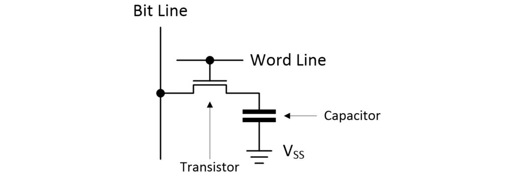
DRAM bit cell (Source: Max Maxfield)
The next level up is an array formed as rows and columns of bit cells. As a simple example, consider a 4×4 array as illustrated below.
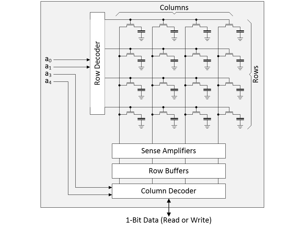
4×4 array of DRAM bit cells (Source: Max Maxfield)
In a real device, the row address might be 16 bits, resulting in 2^16 = 64K rows, while the column address might be 10 bits, resulting in 2^10 = 1K columns. Suppose we wish to perform a read operation. First, we select a row and copy its contents into the row buffers. Next, we use the column address to select the individual bit in which we are interested. This is the bit that will be presented on the DRAM’s external interface.
I once read a “funny” in the Reader’s Digest along the lines of, “You know you’re growing old if, when you bend to tie your shoelace, you look around to see if there’s anything else you can do while you are down there” (it’s not so funny now that I find myself doing this myself). Similarly, since it takes time and energy to power up and access a row—since we already have all the bits from that row copied into the row buffers—it would be advantageous if the way in which we had stored our data meant we could make use of all the bits on the row “while we are here” (we will return to this later).
Moving on… if we wish to create a DRAM with a 4-bit-wide data interface, for example, we will require four such arrays (common DRAM chip interface widths are 4-bits, 8-bits, and 16-bits). A group of arrays like this is called a “Bank” as illustrated in (a) below.
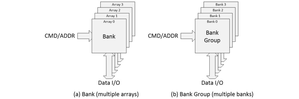
4-array bank (a) and 4-bank group (b) (Source: Max Maxfield)
Multiple banks may be gathered to form a “Bank Group” as illustrated in (b) above. And a DRAM chip may contain multiple Bank Groups as illustrated below.
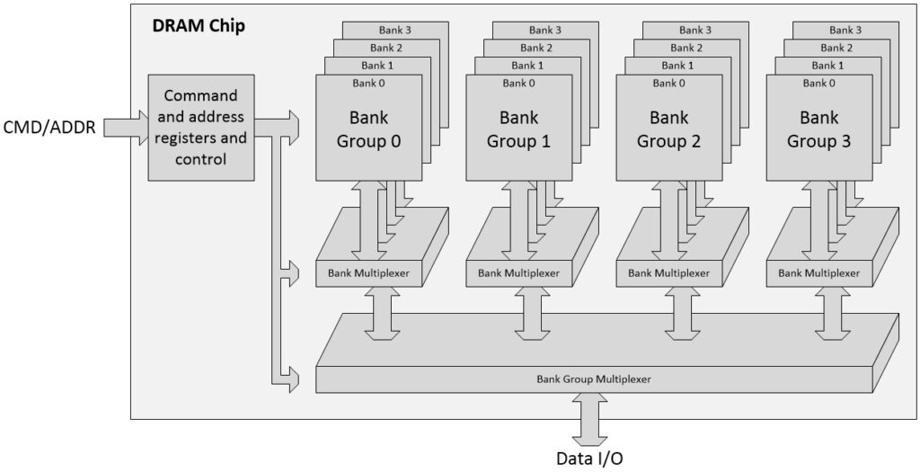
A DRAM chip (Source: Max Maxfield)
Remember that everything we’ve talked about thus far has been based on having simple 4×4 arrays of bit cells and 4-bit deep banks, all resulting in a 4-bit bus being presented at the chip’s external interface (there will also be command and address busses, which are multiplexed together in modern DRAMs).
Earlier, we noted that common DRAM chip interface widths are 4-bits, 8-bits, and 16-bits. Let’s stick with a 4-bit interface. Suppose we wish to work with a 32-bit data bus. We will also need error correction code (ECC) bits. Writing the ECC code at the same time as the payload data is known as “Sideband ECC.” In this case, a 40-bit DDR channel will employ 32 bits for the data and 8 bits for the ECC.
![]()
A Rank of DRAM chips forming a 40-bit channel (Source: Max Maxfield)
The entire row of DRAM chips is known as a “Rank,” and, of course, a memory-guzzling system may boast multiple ranks. The DRAM chips may be mounted directly onto the same printed circuit board (PCB) as the SoC. Alternatively, they can be presented on smaller boards that will be attached to the main board as plug-in modules. The DDR memory controller IP in the SoC can support multiple channels, and the SoC itself may boast multiple such controllers (I’ve heard tell of one humongous SoC that flaunted 20 of Cadence’s DDR controllers—Eeek!).
The great thing about DRAM is that it offers high capacity and low power (relatively speaking, of course). Contrariwise, the big problem with DRAM is that the speed of the bit cells at its core has remained relatively unaffected by process scaling. To be more specific, the speed of bit cells hasn’t changed appreciably in the past 15 to 20 years or so.
Since the core of the DRAM is so slow as compared to the speed of the processors and accelerators on the SoC, the difference is bridged by accessing (reading and writing) lots of information inside the DRAM in parallel and then serializing it at the external interfaces to the devices. This is where all the banks and bank groups come in. While we are powering up and accessing the rows in the arrays forming one bank, we can also be powering up and accessing the rows in the arrays forming another bank.
This is where things start to get complicated. Hashing algorithms may be employed in the SoC interconnect to pseudo-randomize accesses to DDR controller channels (this would need to be configured in the interconnect). Hashing algorithms may also be employed in the DDR controller to pseudo-randomize accesses to the bank groups and banks inside the DRAM chips (this would need to be configured in the controller).
Sitting on top of the hashing (or lurking underneath the hashing, depending on your point of view), is address bit mapping—that is, deciding which bits in the memory address generated by the SoC will be mapped onto channels, ranks, chip IDs, bank groups, bank addresses, row addresses, and column addresses in the real world (whatever that is—“Reality leaves a lot to the imagination,” as John Lennon famously noted).
All this matters! Let’s assume we have two workloads with different memory accessing profiles. The first workload may see significantly higher performance when using a Bank-Row-Column addressing scheme as compared to a Row-Bank-Column scheme. Meanwhile, the second workload may provide dramatically better performance when using the Row-Bank-Column approach. And then things start to get complicated…
THIS IS THE SECOND IMPORTANT BIT: The folks at Cadence have created a library of System Verification IPs (System VIPs). These highly-configurable System VIPs can be used to generate different workload profiles to stress, analyze, optimize, and prove the design. They can be employed in many ways, such as replacing a processor cluster with a System VIP and then monitoring the traffic flow through the interconnect and the DDR controller. These VIPs are complemented by sophisticated analysis tools that allow developers to monitor performance aspects like outstanding transactions (OTs).
The real point of all this is that if we were to take an SoC design that was achieving only 50% of its expected throughput, we might find that simply modifying the configuration parameters associated with one or more of the IPs could return the device to its desired performance. Obviously, it’s better to do this as early as possible in the design phase before we freeze any of the configuration parameters into cold, hard silicon.
THIS IS THE REALLY IMPORTANT BIT: My chums Nick Heaton, who is a Distinguished Engineer at Cadence, and Colin Osborne, who is a Distinguished Engineer at Arm, have written a Performance Cookbook that explains how to understand and optimize the hardware performance of Arm-based SoCs in excruciating exhilarating detail (although this tome focuses on Arm-based SoCs, the tools and techniques are also applicable to RISC-V and other processor-based systems).
This book is so new that, at the time of this writing, it isn’t even available yet, which means I’m not allowed to make mention of the copy I have sitting on my desk singing its siren song in front of me, so I won’t. Suffice it to say that as soon as the book is ready to rock and roll (which could be measured in just hours or days as a I pen these words), this Performance Cookbook link will take you to where you need to go to order a copy.
Meanwhile, while we wait for the book to become available for anyone who isn’t me, what do you think about all of this? Have you had any personal experiences with SoCs that—while functionally operational—failed to live up to their performance expectations?


