


I’ve just been introduced to a solution to a computer memory problem I didn’t even know existed. To be honest, I think I was happier not knowing there was a problem in the first place (“Ignorance is bliss,” as the ancient Latin writer, Publilius Syrus sagely suggested).
When I look back, I’ve had a long and involved relationship with computer memory. As just one example, I recall an incident sometime in the early 1980s when the small company I was working for decided to create a computer system the size of one of today’s larger American fridge-freezers. One day, my boss tasked me with writing a test program to verify the integrity of the memory subsystem.
I no longer recall the underlying memory technology (it was probably some form of semiconductor SRAM, but it could have been magnetic core store for all I know). All I do remember is that (a) the memory subsystem occupied a filing cabinet-sized drawer, (b) it weighed in at a whopping 50 pounds or so, and (c) it presented itself as a single address space from 0x0000 to 0xFFFF. That’s right, a staggering 64K words of memory, where each word was 32-bits wide.
I was young and foolish, and I’d never done anything like this before (now I’m old and foolish, and I will do my utmost to never do anything like it again), so I started off simply by writing 0x55555555 (01010101…) into address 0x0000, reading it back, writing 0xAAAAAAAA (10101010…) into address 0x0000, reading that back, and then repeating this test for all of the remaining addresses.
I’d just performed my first run and received a “thumbs up” message from my program when my boss ambled into the lab to see how I was getting on. “That’s interesting,” he said when I proudly showed him the result, “because the memory is sitting on the table behind you.”
“Oh dear,” I thought to myself (or words to that effect). After my boss had glanced at my code, he explained that my problem was that there was sufficient capacitance on the data bus to retain the value I’d just written long enough for me to read it back again. I felt like a fool (which proved to be good practice for the future). You can read more about all this in Designus Maximus Unleashed (Banned in Alabama). But we digress…
One thing that was nice about the early 1980s was that we didn’t worry about nefarious folks infiltrating our systems over the network, because we didn’t have a network. The military had networks, but their usage by companies and corporations was not the norm at that time.
These days, of course, we have networks of networks, and bad actors abound, from individuals to nation states, all trying to gain access to our data and—if possible—take control of our systems.
In the case of a server used in the cloud, any processor on-chip memory is implemented using Static Random-Access Memory (SRAM), while the server’s main on-board memory is implemented in Double Data Rate (DDR) Dynamic Random-Access Memory (DRAM).
DRAM offers many advantages, including low cost, low power consumption, and high capacity (all in comparison to other memory technologies like SRAM). DRAM also offers high performance, although the way in which this is achieved is outside the scope of this column. On the downside, DRAM also presents attack vectors that provide the potential for cybercriminals to crack open a system and feast on its tasty insides.
I was just chatting with Steven Woo, who is a Fellow and Distinguished Inventor at Rambus, and Wendy Elsasser, who is Technical Director Research Science at Rambus Labs. Steven and Wendy were kind enough to introduce me to a DRAM security exploit called rowhammer (or row hammer) of which I was previously (blissfully) unaware.
To wrap our brains around this, we need to start with a high-level understanding of what’s inside a DRAM chip. The fundamental building block of a DRAM is the bit cell, which employs a capacitor and a transistor to store a single bit of data.
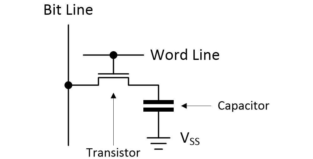
DRAM bit cell (Source: Max Maxfield)
The next level up is an array formed by rows and columns of bit cells. As a simple example, consider a 4×4 array as illustrated below.
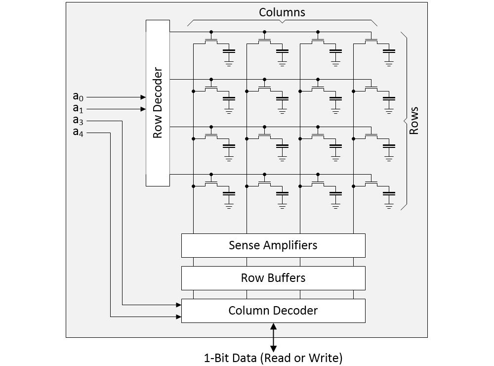
4×4 array of DRAM bit cells (Source: Max Maxfield)
In a real device, the row address might be 16 bits resulting in 2^16 = 64K rows, while the column address might be 10 bits resulting in 2^10 = 1K columns. Suppose we wish to perform a read operation. First, we select a row and copy its contents into the row buffers. Next, we use the column address to select the individual bit in which we are interested. This is the bit that will be presented on the DRAM’s external interface. Of course, this means that if we wish to create a DRAM with a 4-bit wide data interface, for example, we will require four such arrays (common DRAM chip interface widths are 4-bits, 8-bits, and 16-bits).
This “stack” of arrays is called a “bank.” A DRAM chip may contain a “stack” of banks, which would be referred to as a “bank group.” It gets better (or worse, depending on your point of view), because the same chip can contain multiple bank groups, but that’s not something we need to worry about here.
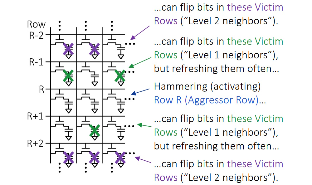
What we do need to worry about is rowhammer. One of the unintended and undesirable side effects of the DRAM architecture is that bit cells in adjacent rows can interact electrically between themselves by leaking their charges, possibly changing the contents of nearby cells that were not addressed in the original memory access.
Obviously, a single access to a row won’t flip any of the bits in an adjacent row, otherwise DRAM would be useless. However, specially crafted memory access patterns that rapidly and repeatedly activate (“hammer”) the same memory rows with 00000… or 11111…. values can change the contents of nearby memory rows that were not addressed in the original memory accesses.
How many is “numerous”? Ah, there’s the rub. Known as the hammer count (HC), this value has fallen by more than an order of magnitude over the past decade. A couple of DRAM generations ago, we were talking about HCs of 15K to 50K hits before seeing any bits flipping in adjacent rows. The HC is falling by a factor of four for each new generation of devices. It’s in the vicinity of 4.5K to 15K with the current generation, and it’s anticipated to fall to around 1K to 3K in the next generation.
Furthermore, in addition to the traditional form of rowhammer attack, we now need to prepare ourselves to deal with half-double attacks. Let’s start with a traditional rowhammer attack on row R (the “aggressor row”) as illustrated below. This attack may result in bits flopping in “victim rows” (R-1) and (R+1).
Different types of rowhammer attack (Source: Rambus)
Now, it’s important to remember that DRAMs are dumb devices. All the intelligence is contained in external DDR controllers and any higher-level processors. Suppose that a controller (or a higher-level processor) decides that a rowhammer attack may be taking place. One way to mitigate this is to perform additional refreshes on the victim rows to restore their bit cell contents to their full values. The idea between the half-double form of rowhammer attack is that by persuading the host system to repeatedly refresh victim rows (R-1) and (R+1), these victims eventually become aggressors with respect to their neighboring rows at (R-2) and (R+2).
Yet another consideration is how the controllers and higher-level processors detect a rowhammer attack in the first place. Even something as simple as keeping a count of the number of consecutive accesses (or periodic bunches of accesses) to the same row is problematic, not least that these numbers need to be stored somewhere.
Have you read the science fiction book Dune and/or seen the Dune 1 (2021) and Dune 2 (2024) movies? If so, you will know that if you go for a wander in the Dune desert using your normal gait, you will attract the attention of giant sand worms. Trust me; if there’s one thing you don’t want to do, it’s to attract the attention of giant sand worms. Thus, the natives of Dune employ a technique called the sandwalk, which is a rhythmless way of walking that emulates the natural sounds of the desert.
Similarly, the creators of rowhammer attacks create patterns of memory accesses that are designed to fool rowhammer detection (and mitigation) algorithms. As a simple example, they might employ decoy rows around the targeted hammer row(s), and then use pseudo-random patterns to occasionally hit the decoy rows while predominantly hammering the targeted row(s).
Before we proceed, we should take a few moments to remind ourselves why the perpetrators of rowhammer attacks are doing so in the first place. Some attacks are just to see what mischief people can cause. Others are intended to gain privileged access to areas in memory to which they weren’t supposed to have access. For example, the Project Zero team at Google penned an interesting paper: Exploiting the DRAM Rowhammer Bug to Gain Kernel Privileges.
But wait, there’s more. In the same way that “No man is an island,” as John Donne famously wrote, so too DRAM chips are rarely used in isolation. Instead, a group of chips are presented in a row called a “rank” on the motherboard or a memory module. Assume we are working with 8-bit wide DRAM devices, and we wish to implement a 64-bit wide memory bus. In this case, we will need eight DRAM devices in our rank. If we also assume we are using a sideband form of error correction code (ECC), then we will require a ninth device as illustrated below.
![]()
Rank of DRAM chips (Source: Max Maxfield)
This is a very stylized and simplistic depiction. For example, there may be multiple ranks. Also, I’ve not shown the command and address buses (these are multiplexed together). The important thing to note in the context of these discussions is that (a) all the control signals (command, address, chip-select, etc.) are identical for all DRAMs in the rank and (b) the chips themselves are functionally identical as seen by the outside world (e.g., there are no pins on the chip we can use to identify one chip from another).
With respect to point (a), hammering address 0x0001 may flip bits in row addresses 0x0000 and 0x0002, and it may do this to all the chips forming the rank. What about the ECC? Well, this is typically capable of detecting and correcting a single bit flip error and detecting (but not correcting) two bit-flip errors. However, since the address presented to the DRAM chips is identical for each chip, any access made by the external controller will affect the same row in all the DRAMs. Thus, a hammer attack on a specific row can flip multiple bits in multiple DRAMs, thereby overwhelming the ECC, resulting in uncorrectable errors and, worse, so-called “silent data corruption” (the system can’t even tell that the data has been corrupted).
With respect to point (b), you may have heard of pins on the DRAM package being used to implement something called a Chip ID, but that’s different to what we are talking about here. In the Chip ID case, each DRAM package contains multiple chips in the form of stacked die, so the Chip ID is used to identify the die of interest. Thus, the Chip ID field forms part of the address, and its value is identical for each of the DRAM devices forming the rank.
This is where the clever folks at Rambus come into the picture. They set themselves a goal that the system should continue to run following a rowhammer attack even if all the bits in neighboring victim rows flip. Also, they wanted their solution to have no performance impact on DRAM accesses, and they wanted their solution to be compatible with other rowhammer mitigation techniques (row tracking, probabilistic selection…).
Their solution is called RAMPART, which stands for Row Address Map Permutation And Reassignment Technique (phew!). I’m informed that this novel and unique approach to addressing rowhammering for DRAM offers up to 17 orders of magnitude better resistance to such data corruption attacks. O-M-G! That’s a lot of orders of magnitude!
RAMPART takes a bit of wrapping one’s brain around (well, it did for me) but—notwithstanding what I said earlier—suppose there was some way for each DRAM chip to have some form of identity, such that DRAM 0, 1, 2 etc. in the illustration above are “aware” that they are numbered 0, 1, 2 etc. In fact, DDR5 devices have a field within the mode register space that can be used to implement such an ID.
Now suppose that this ID is used inside the device to remap addresses in some way. Just to provide an off-the-cuff remapping example, also suppose that the address provided by the controller is circularly rotated left by n bits, where n = (2 x the ID number of the device). In this case, assuming the external controller is writing to address 0x0001 as before, then this will be remapped as follows:
Chip 0 will circularly rotate 0x0001 left by (2 x 0) = 0 bits, which means the address being written to in Chip 0 will remain 0x0001, and the rows being hammered in Chip 0 will be 0x0000 and 0x0002, as before. By comparison, Chip 1 will circularly rotate address 0x0001 left by (2 x 1) = 2 bits to be 0x0004, which means the rows being hammered in Chip 1 will be 0x0003 and 0x0005. Similarly, Chip 2 will circularly rotate 0x0001 left by (2 x 2) = 4 bits to be 0x0010, which means the rows being hammered in Chip 2 will be 0x000F and 0x0011. And so forth.
Now, suppose that following the rowhammer attack, we perform a read on address 0x0002. Chip 0 will circularly rotate 0x0002 left by (2 x 0) = 0 bits, which is one of the rows that was hammered by the attack. However, Chip 1 will circularly rotate 0x0002 left by (2 x 1) = 2 bits to be 0x0008, which wasn’t one of the rows that was hammered in this chip. Similarly, Chip 2 will circularly rotate 0x0002 left by (2 x 2) = 4 bits to be 0x0020, which wasn’t one of the rows that was hammered in this chip. And so forth.
The bottom line is that for any victim row address generated by the DDR controller, RAMPART will confine bit flips to a single DRAM device. Like I say, this does take a bit of time to wrap your brain around, and the real remapping algorithm isn’t the one I showed here, but the underlying concept is rather clever. One super-cool thing is that DRAMs already contain an internal row-remapping capability to handle bad rows (e.g., defective rows from when the device was manufactured), and this can easily be extended to implement RAMPART. Another super-cool thing is that the existing ECC will continue to work following a rowhammer attack. Ha! Take that, cyberslime!
As usual, there’s a lot more to all this than I’ve been able to cover here. Happily, if you want to learn more, the folks at Rambus have written a robust research paper for your delectation and delight: RAMPART: Rowhammer Mitigation and Repair for Server Memory Systems. As for me, I’m going to apply an icepack to my overheated noggin. In the meantime, as always, I welcome your comments and questions.


A story about a magic switch comes to mind:🙄
https://github.com/PDP-10/its/issues/1232
That is a very interesting story — thanks for sharing
ROwhammer is bullshit.
Criminally crappy HW implementation is being sold as solid design and then they portray particula design access patterns as somehow inherently nefarious.🙄
DRAM cells SHOULD endure any possible access pattern fo the cells in its vicinity no matter what.
If there is any signal degradation, it should have been well within safety margins and it should be taken care of by the regular refresh cycles.
But ofcourse DRAM manufacturers are under pressure to “innovate” from quarter to quarter, their “innovation” is endless circumcision of vertical DRAM capacitors and their mutual isolation.
Besides DRAM controllers have that covered lately AFAIK they can detect aggressive row hammering and they simply refresh adjacent ones.🙄
But in general, this is just mostly about industry beancounters silently eroding the foundation ofwhole computing industry – ability to store data reliably.
FFS, DRAM HAS RANDOM ACCESS IN ITS FRIGGIN ACRONYM.
So, all the sudden we have to access it like walking through the minefield ?!?
“AFAIK they can detect aggressive row hammering and they simply refresh adjacent ones”
But it’s the refreshing of the adjacent rows than can constitute another attack in its own right.
And when geometries shrink and you can cause a rowhammer induced failure with only 1000 consecutive writes…
On the other hand, I do see your point.
Designing semiconductors, including DRAM, is a careful balancing act between size, cost, power, performance and more. New generations of semiconductors leverage smaller process technologies, introducing effects that compound these challenges. In DRAM, smaller geometries result in physical challenges such as reduced cell-to-cell spacing and increased electromagnetic interactions between cells.
Subsequently, scaling has introduced effects that have increased the susceptibility of activation induced bit flips like RowHammer. Addressing these challenges will require continued collaboration across the industry.
“And when geometries shrink and you can cause a rowhammer induced failure with only 1000 consecutive writes…”
Failure isn’t induced, it IS INHERENT.
IOW, we are being sold DEFECTIVE products.
And rowhammer stuff is just one example. There are plenty of cases where memory is just tested not across all legal conditions, but EXPECTED conditions in typical use.
One example: even from DDR3 times (and still today with latest gen!) one can hear from manufaturers that they don’t know if it should work at say x00MHz, because no one ever tested it…
T;DR: they don’t give a shit. All that matters is that they manage to keep the thing at typical customer’s premise for 2 years and then, if something goes wrong and it can’t be blamed on customer, well it’s time for an upgrade anyway…