

I grew up in the age of 8-bit microprocessor units (MPUs). Consider the MOS Technology 6502, which was introduced in 1975, for example. This was the year I graduated from high school. I was 18 years old, bright-eyed, bushy-tailed, and totally clueless as to the ways of the world (to know me was to love me—this was long before I became the curmudgeonly, battered, bitter, broken man you see before you now).
In addition to its 8-bit data bus, the 6502 had a 16-bit data bus, thereby allowing it to address 64kB of memory. Based on NMOS technology, the 6502 was manufactured at the 8µm process node and presented in a 40-pin dual in-line package (DIP).
The 6502’s minimalist internal register offerings included one 8-bit accumulator register (A), two 8-bit index registers (X and Y), 7 status flag bits, an 8-bit stack pointer (S), and a 16-bit program counter (PC). Although it could be clocked at a higher rate, most systems with which I was familiar used a ~1MHz clock.
As an aside, have you ever wondered as to the origin of the term “flag” in the context of a status bit? I always thought of this as being a metaphorical construct based on the use of flags for signaling, like the flag semaphore system employed by my granddad when he was in the British Royal Navy during WWI and WWII. I never considered that status flags in computers might once have had a physical incarnation.
Well, I’m currently reading Computer Architecture from the Stone Age to the Quantum Age by Charles Fox. This is an awesome book. I’ve long been familiar with Charles Babbage’s proposal for a mechanical computer called the Analytical Steam Engine circa 1837. I knew it had a mechanical central processing unit CPU) and a mechanical random-access memory (RAM), but I’ve never been introduced to its inner workings… until now. I now know that this bodacious beauty was intended to work with 50-digit decimal numbers. Also, it had a mechanical data bus connecting the CPU and RAM. Also, the CPU contained mechanical registers, a mechanical arithmetic logic unit (ALU), and a mechanical control unit (fetch, decode, execute, store). More importantly, I now have a much better idea as to how all these functions were physically implemented and how they worked together (and I’m only on Page 83 of 436!)
It was while perusing and pondering the section on the ALU that I ran across the following: “In addition to sending the result to an output register, some ALU operations can also set a single status flag as an extra, side-effect output. The status flag in the Analytical Engine is a single mechanical lever that is either in the up (1) or down (0) position. It might have had an actual red fabric flag on it to visually alert human as well as mechanical observers that ‘something of interest just happened’ in the ALU.” I LOVE learning stuff like this!
As one more aside before we plunge headfirst into the fray with gusto and abandon (and—as always—aplomb), let’s remind ourselves that the Commodore 64, also known as the C64, which was introduced in 1982 and which has been listed in the Guinness World Records as the highest-selling single computer model of all time, was based on the 6510 8-bit processor (a slightly modified version of the 6502) running at 1,023 MHz (NTSC version) or 0.985MHz (PAL version). The reasons we are reminding ourselves of this are (a) Retro Games offers THEC64, which is a full-size modern replica of the original C64 (implemented using an FPGA, running the original instruction set, but with support for a USB mouse and HDMI output) pre-loaded with 64 retro games, fully programmable in BASIC, (b) I have one of these beauties, and (c) my friend Jonny Doin (who is based in Brazil and who reads all the articles here on EEJournal) doesn’t, which means he will be gnashing his teeth and rending his garb when he reads these words [“Hi Jonny!” 🙂 ]
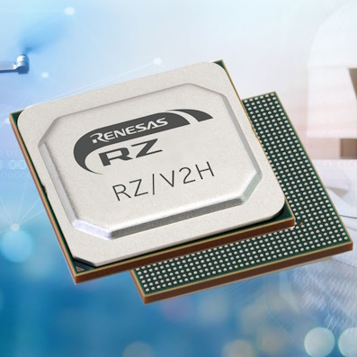
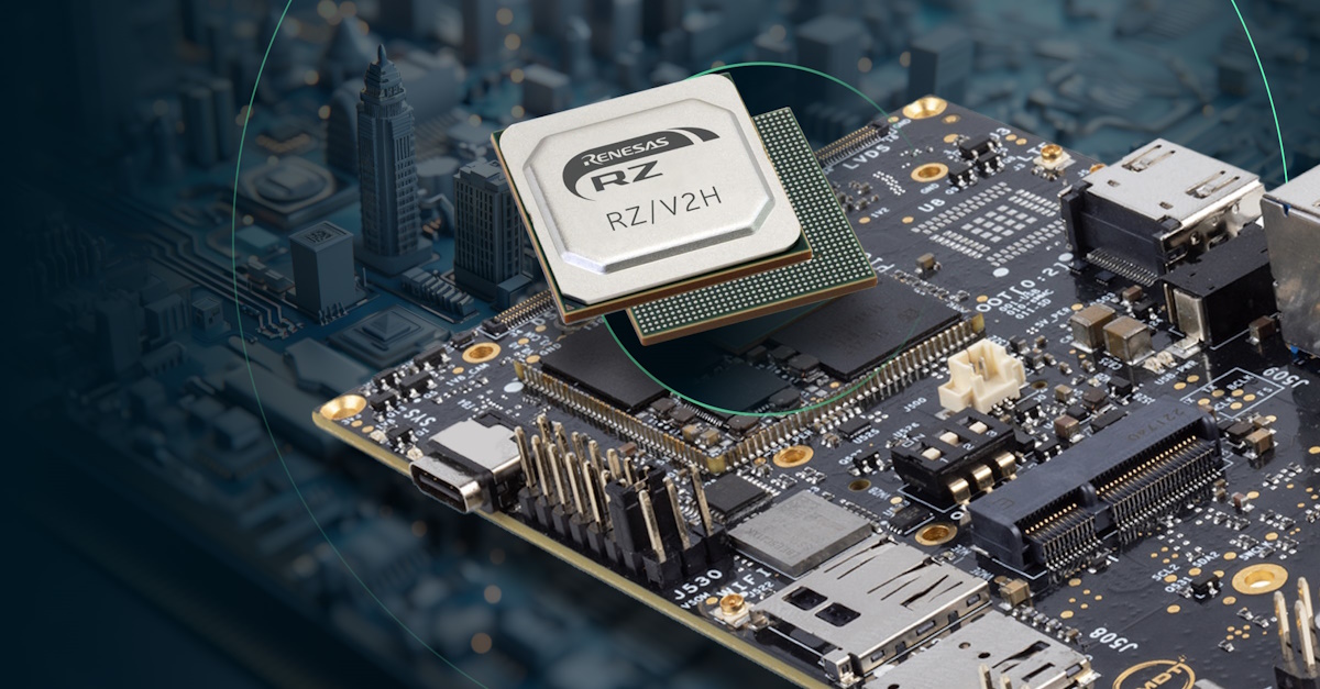
The reason for my current cogitations and ruminations is that I was just chatting with Brian Witzen, who is the Business Development Manager for RZ/V products at Renesas Electronics. These devices are focused (no pun intended) on vision applications in the edge embedded application space. Brian was bringing me up to date with the recently introduced RZ/V2H MPU. With its integrated artificial intelligence (AI) accelerator, this MPU achieves high power efficiency coupled with real-time performance.
 The RZ/V2H MPU achieves high power efficiency coupled with real-time performance (Source: Renesas)
Now, you could say, “But lots of MPU manufacturers boast high power efficiency with real-time performance.” To which I would answer, “Yes, that’s true, but it all depends on what you are trying to do.” You can certainly use a variety of MPUs for simple AI vision inferencing tasks, but you are going to have to search long and hard for one that can perform ResNet50 at 830 frames-per-second (fps).
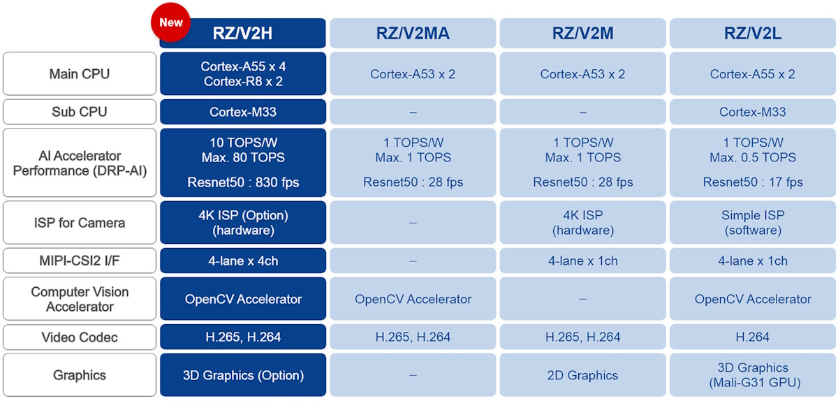 64-bit RZ/V MPU Lineup for Vision AI (Source: Renesas)
The lineup above compares the existing RZ/V2L, RZ/V2M, and RZ/V2MA MPUs with the new RZ/V2H family. Feast your orbs on these facts and figures. A quad Arm Cortex-A55, a dual Cortex-R8 for real-time operations, and a humble Cortex-M33 to do the grunt work no one else wants to do (I know how it feels). And then there’s the DRP-AI—the AI accelerator—providing 10 trillion (tera) operations per second (TOPS) per watt, with a max of 80 TOPS. “Oh, my giddy aunt,” is all I can say (I’m sorry, Auntie Barbara; I didn’t mean to take your name in vain).
One thing I’d like to point out is that some chip vendors announce a product, raising our excitement and expectations, and then cruelly crush our spirits when they inform us that the part in question won’t become available for another year (“or two… three at the most”). That’s not the way the folks at Renesas roll. When they make an MPU public, it’s already in production. In the case of the new RZ/V2H, for example, although this was formally announced on 29 February 2024, it was actually put into production in December 2023, since which time the guys and gals at Renesas have been building up stocks and ensuring support functions like associated evaluation kits (EVKs) are ready to rock and roll. Personally, I find this to be a very welcome breath of fresh air, as it were.
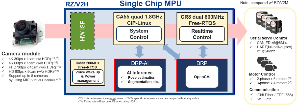 High-level RZ/V2H block diagram (Source: Renesas)
I’m not going to get into the CA55, CR8, and CM33 processors. We all know what they are capable of. Instead, let’s remind ourselves that—a few years ago—the chaps and chapesses at Renesas came up with something they call the dynamically reconfigurable processor (DRP). We can think of this as a small arithmetic unit or programmable arithmetic unit fabric—a bit like programmable FPGA fabric (but not really)—that can be totally reconfigured on every clock cycle. Well, the DRP-AI includes a bunch of multiply-accumulate (MAC) functions, thereby making it like a DRP that’s been working out on steroids.
We should perhaps note that the RZ/V2H employs the third generation of the DRP-AI. Earlier versions were based on 16-bit dense floating-point (FP) quantization. The new engine is based on 8-bit integer quantization, either dense or pruned/sparse.
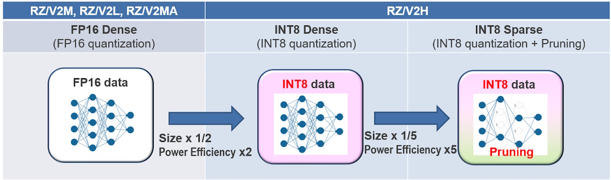 DRP-AI Evolutionary features (Source: Renesas)
On the one hand, moving from 16-bit floating-point to 8-bit integer does cause a couple of percent loss in accuracy, but the 10X boost to power efficiency makes this tradeoff well worthwhile. It’s important to remember that AI inferencing is always going to be probabilistic. Does it really matter if your 16-bit floating-point-based inferencing engine says, “I’m 97% convinced we’re looking at a chicken” while your 8-bit integer-based engine says, “I’m 95% convinced we’re looking at a chicken”? “No!” I cry, “It’s a CHICKEN!”
One thing that’s not shown here is the memory, which is presented as two 32-bit channels of external low power DDR4 (LPDDR4). Remember that this is a microprocessor/MPU with external memory and not a microcontroller/MCU with internal memory.
I did a bit of rooting around to discover that the RZ/V2H uses DDR memory controller intellectual property (IP) from Cadence. This is of particular interest to me because today’s IPs (processors, DDR controllers, on-chip interconnect, etc.) are incredibly configurable, and tuning them to achieve optimal performance for specific software workloads is no trivial task (I will be talking about this in more depth in a future column).
So, where can we expect to see (yes, pun intended) these vision processors being deployed? Well, the target markets and applications are largely limited only by our imaginations.
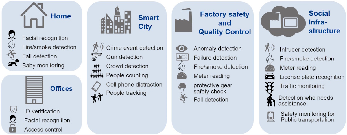 Example markets and applications (Source: Renesas)
As I previously noted—and as illustrated below—RZ/V2H evaluation kits (EVKs) are already available for our delectation and delight.
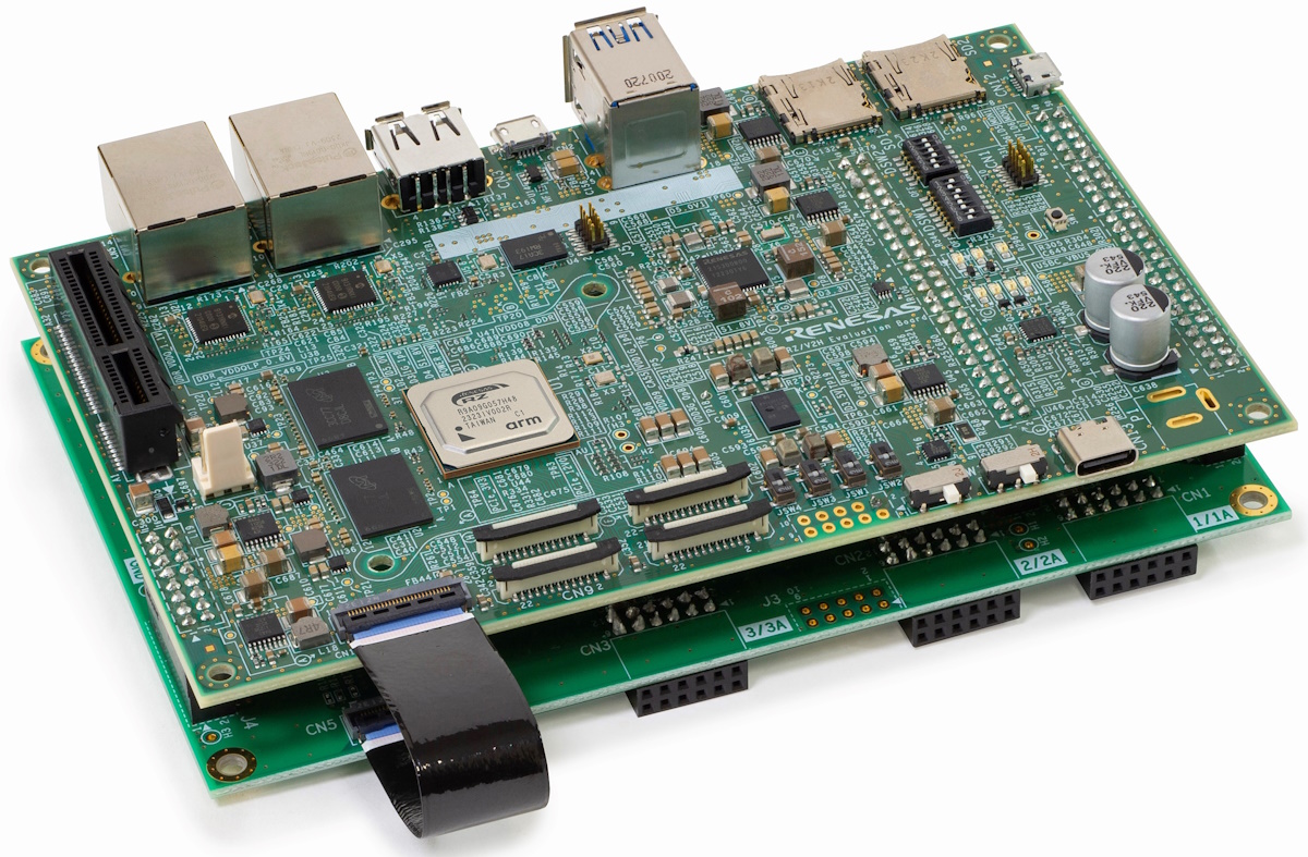 RZ/V2H evaluation kit (Source: Renesas)
And, lest you doubted me when I told you that RZ/V2H devices are already available for us to start using in our super-spiffy next-generation products, I just saw an announcement from IMD Technologies (IMDT)—a renowned provider of cutting-edge vision and AI-powered products and systems—that they’ve already announced a new line of power-efficient, cost-effective, and ready-to-use system-on-module (SOM) and single-board-computer (SBC) solutions—their V2H SOM series—that’s based on Renesas RZ/V2H MPUs. Wow, that was fast!
 Renesas RZ/V2H MPU powers IMDT SOM (Source: IMDT)
As usual, I’m left contemplating how far we’ve come over the past ~50 years from the days of the 6502 microprocessor and the C64 home computer to the RZ/V2H AI MPU. I’m almost fearful to think where we may find ourselves technology-wise say 50 years in the future. What say you? Do you have any thoughts you’d care to share on any of this?


