


Today we bring two stories about memory. One is business-model oriented; the other is about technology. We’ll take those two in order.
Competing with Free
What do you do when a product that you sell suddenly becomes available for free elsewhere? Of course, we’ve seen this in a number of contexts (RIP Netscape), but in this case, we’re talking about SRAM. Good SRAM is critical to a good design (“good” being suitably vague), so it definitely has value. Problem is, foundries now have proprietary versions in their libraries that their customers can use without buying separate SRAM IP.
So, if you’re a small company selling SRAM IP, how the heck do you compete with that? It’s not that SRAM suddenly has no value, but foundries have other sources of income, so they can give this away to attract customers. SRAM IP vendors have no such fallback income to make up for lost SRAM income. So what do you do? Sell only highly differentiated SRAM? Start making something besides SRAM? Give up completely?
The first option is the classic MBA directive: make your SRAM compelling enough that people will pay for it even in the face of free versions that aren’t quite so tricked out. But how much are differentiating features worth? We all know from buying cars that, for instance, an option for leather seats is one that many people will forego, thinking, “It’s nice to have, but I’m not paying extra for it.” Is that what happens to differentiated SRAM?
One company in particular, SureCore, is taking the gamble that, yes, there are customers willing to pay for SRAM features that aren’t available in free versions. We looked at SureCore a few years ago, digging into their approach to reducing dynamic power. That’s a good thing, but is it enough?
I talked with their CEO at the recent DAC convention, and he went through the larger range of possible customizations available as well as their engagement model. Dynamic power is but one way an SRAM can be differentiated. They also provide:
- Access feature options, like byte write, masking, and different sleep modes;
- Flexibility on the number of read, write, or read/write ports as well as the ability to make some of the ports slower (presumably reducing area) and allowing burst access as an option;
- Test infrastructure (design-for-test, or DfT);
- In addition to their PowerMiser dynamic power reduction technology (see link above), they can also lower static power by eliminating pre-charge and letting the bit lines float (they go to about 80% of VDD);
- An “EverOn” feature that lets you keep the SRAM in a low-voltage retention state even when using the memory. The bit and word lines are segmented with individual VDDs, and those VDDs are temporarily boosted for read/write operations only on the segments that need them, leaving the rest in a retention state. The whole thing can operate over a wide voltage range.
That’s a pretty broad set of potential added-value features. Is it enough to generate interest?
According to SureCore, they have achieved some traction. But my sense is that the custom features being used will need to be strategic to product value, since the engagement model is long.
- Once the feature set and target technology and foundry are established, extensive verification is needed to evaluate how the memory responds given process variations. How big is the viable window? They use Solido tools for this part of the verification, focusing first on critical circuits like sense amps. From there, they then automate the checkout of the rest of the circuit.
- At this point, however, the analysis isn’t enough to allow the IP to be inserted into a larger SoC design. Test chips are required first, and that can be a 9-month process to complete.
- This process must be repeated if the foundry or process node is changed.
- In addition, the investment to purchase a custom SRAM is “substantial.”
So the customer really has to want this. And I’m going to assume that this kind of time and money won’t be spent on a one-off tactical application, but rather that it will need to feature in a number of products in order to amortize the effort.
So what kind of application might warrant this focus on differentiation? We discussed that, and it’s really a new-market thing. Obvious opportunities are artificial intelligence/machine learning and virtual reality. These are fluid new markets with lots of competition, so companies need critical secret-sauce technology if they want to stand out. That’s where SureCore can win: when they’re helping a newcomer to establish their secret sauce.
We talked about potential other threats, and the only one that may or may not materialize is MRAM – if it can achieve the performance that everyone has been looking for. Given that foundries haven’t taken standard 6T SRAM off of their roadmaps, SureCore still sees plenty of opportunity ahead.
Speaking of MRAM…
Meanwhile, Imec made an MRAM announcement recently that’s worth noting. Traditional spin-torque transfer (STT) MRAM has hit something of a brick wall with respect to speed. To make it fast enough to compete with SRAM, the data retention suffers badly. So a new type of MRAM, called spin-orbit transfer (SOT), is in development.
We looked at it in more detail a year ago, but the executive summary is that older MRAM used current in the same direction both to program and read a cell – meaning that lots of current for a fast write operation affects cell reliability and data retention. SOT MRAM programs uses an in-plane current that runs across the cell rather than through the tunnel junction, allowing a low-current write that still operates below 1 ns.
But there’s been a catch: when setting the tunnel state, there’s some uncertainty as to which direction it will program. An external magnetic field helps to force the correct direction. And that’s a pain in the kiester. Do you mount a magnet outside the package? Inside the package? It’s just not a clean, easy thing to do.
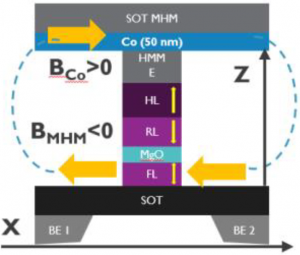
Imec has successfully tested an idea that integrates well into the process flow without compromising a small cell size. They refer to the area through which the in-plane programming current runs as the track, and the rectangular footprint of that track is established by a metal hardmask (MHM). Traditionally, this MHM has consisted of TiN. What’s different here is that an additional 50-nm layer of cobalt is deposited as part of a composite MHM, and that cobalt can establish the needed static field.
The following is a drawing of the cell stack, followed further down by a TEM image of the cell cross-section.
(Image copyright Imec, used by permission)
There are a bunch of acronyms that we should define (in addition to the ones we’ve already seen) to help navigate the drawings. Starting from the top of the stack above, we have:
- Spin-orbit transfer metal hard mask. This is a little confusing because, in the drawing, we have this layer over the cobalt layer, while in the TEM image, the cobalt is the MHM under the TiN. In reality, there’s one MHM made up of a layer of cobalt and then the TiN above that. So combine the two images.
- HM_ME: hardmask memory element. This is used to pattern the actual magnetic tunnel junction.
- HL: I’m actually not sure what the letters stand for, but this is a synthetic antiferromagnet (SAF), which is used to pin the reference layer.
- RL: that’s the refernece layer (with a fixed orientation used for “comparison” with the free layer).
- MgO: this is the material used for the magnetic tunnel junction (MTJ).
- FL: free layer; this is the layer whose orientation gets programmed to set the cell state.
- SOT layer: this is where the programming current runs, connect by tungsten vias to the…
- BE: bottom electrode. The top electrode is the copper interconnect.
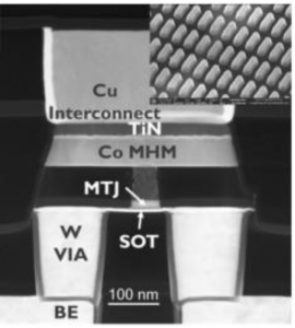
(Image copyright Imec, used by permission)
You can also see here the distinction between the track – the wider area defined by the MHM – and the actual cell junction, defined by the HM_ME.
The process flow is summarized in the following figure.
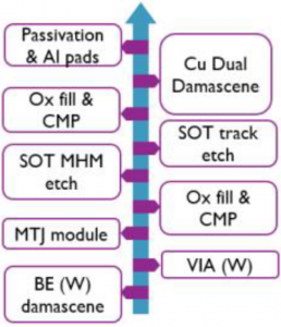
(Image copyright Imec, used by permission)
There’s still one open question here: how does the cobalt get magnetized? If a metal is deposited with no other effort taken, the atoms are likely be randomly oriented, resulting in no discernible net magnetic field. So, somehow, we need to establish a magnetic field in the deposited cobalt. No such step is shown in the process flow above, and I didn’t see anything in the paper. So I asked Imec.
And, as usual, this took me deeper into magnetics than I was expecting. (I was an electrical engineer, not a magnetic engineer, after all!) First of all, it turns out that things work differently with thin films than they do with bulk materials. Second, they rely on something called shape anisotropy to help. Anisotropic shapes – rectangles instead of squares, ellipses instead of circles – have a so-called easy axis and a hard axis. The longer axis is easier to magnetize as it results in lower energy. You can magnetize across the hard axis, but it’s, well, harder to do.
So the rectangular track provides the anisotropy needed to ease the preferential polarization. On its own, the thing could polarize in either direction along the easy axis – and yet that’s the whole problem we’re trying to solve with this MHM. Magnetizing the cobalt in fab is what breaks that symmetry, and, without giving away how they did it, Imec said that you could deposit the cobalt in the presence of a magnetic field or have a separate magnetization step at the end of the process.
We’ll see whether this or something similar becomes the Great Enabler that pushes SOT-MRAM into the market – posing a threat to embedded SRAM and embedded flash in microcontrollers and systems-on-chip.
More info:
Manufacturable 300mm platform solution for Field-Free Switching SOT-MRAM (PDF)
Sourcing credit:
Paul Wells, CEO, SureCore
Kevin Garello, R&D senior scientist specializing in memory devices, Imec


What do you think of SureCore’s approach to custom SRAM? And do you see Imec’s metal hardmask as a game changer for SOT-MRAM?