


SRAM is everywhere these days, mostly in its embedded form. As memory gets relatively cheaper or denser, it becomes more desirable to pack robust bunches of it into SoCs.
But let’s face it: standard SRAMs are a pain in the byte. They’re big, requiring 6 (or even 8) transistors for each bit of memory stored. And they’re power hogs, relatively speaking. So why do we love them so much? Because they’re fast, of course.
The 6T SRAM bit cell has been standard fare for many, many years, far outlasting other types of circuits. It’s one of the first cells to be proven on a new technology, where it’s lovingly hand-drawn, given permission to violate lots of rules that other circuits would have to obey, and tested exhaustively to prove that it works – rule violations notwithstanding – across all corners. And then the foundry jealously guards it.
But some cracks have appeared in the pedestal upon which we’ve placed the 6T static memory. We saw one example with a 1-T memory from Zeno at the beginning of the year. Since then, there have been more rumblings. So today we look at two deviations from the norm, very different from each other, but both attempting to address some of the limitations we’ve had to live with in order to merit SRAM speeds in our systems.
Breaking the Bit Line
We start with an SRAM IP company called SureCore. Their goal is to reduce power – dynamic power in particular. Yeah, they’d like to reduce static power as well, but that’s pretty much a function of leakage, which is pretty much a function of the underlying technology – something SureCore can’t control. So they go with dynamic power reduction.
They have some ideas on a lower-power bit cell, but their general concern is that fabs don’t like monkeying with that bit cell on which they’ve spent so much time and energy. It’s not clear whether they’ll pursue that angle, but their main thrust has been to leave the bit cell alone, focusing instead on the architecture. In particular, they found that the bit line is a major participant in the consuming of energy. And so they made a change that, like any improvement, involves tradeoffs, but that they say provides a 50% reduction in dynamic power for the memory.
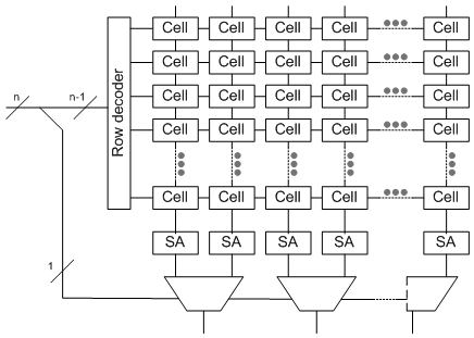
As a reminder, a bit line is the output of the memory array (but not the overall memory). The address is the input, more or less, and much of that address drives the word line – that is to say, the row of the array. The bit line is then the column, although there are often more columns than outputs from the overall memory, so the bit lines have to be muxed into outputs, and the remaining part of the address (the bits not used for the row address) drives those muxes. For reference, a super-abstracted array is shown below, with 2:1 muxes on the bit lines – that is, one bit of the address determines which bit line will be read. (Note that “SA” stands for “sense amp.”)
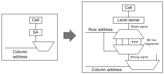
The change SureCore has made is to power down the bit line substantially. Problem is, on its own, this bit-line-lite wouldn’t be powerful enough to drive the follow-on circuits (at least not with any kind of performance). So they’ve added a second stage that acts as a higher-power bit line, except that they’ve split that second stage up into 32-bit (or 64-bit – your choice) segments. Each of these is much faster than a full bit line, and it has the power to drive the signal on. But because this second stage isn’t dragging along the capacitance of a long line attached to bit cells, it’s both faster and lower power.
In fact, in my further super-abstracted rendition of what this might look like (below), this arrangement behaves as if the true bit line is being fed into a demux fed by the row address. All but 5 (or 6) of the row address bits would select a line to use as the output. It might look odd to have a demux then followed immediately by a mux, with both decoded the same way; the point is increased drive. (To be clear, this is my abstraction, don’t assume that their actual implementation looks exactly like this – I’m not privy to their circuits.)
The cost of this power savings comes as a 20-30% hit in the top possible speed and as a 5-10% increase in the size of the memory. It’s available on 40ULP and 28 FD-SOI processes.
Using Dynamic Memory for Static
The next new take on SRAM is a surprising one: replacing the static bit cell with a dynamic one. Bet you didn’t see that coming. This is Mentor Graphics’ coolSRAM-1T approach.
But here’s the deal: they’re doing this not with a process that uses the usual DRAM process modules that can be plugged into a CMOS process, but with only that standard CMOS process – no new modules required. That would mean no vertical transistors or buried word lines or MESH (extra mechanical support) complications. It also operates like an SRAM – none of that RAS/CAS nonsense.
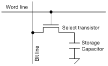
The basic operation retains some of the characteristics of DRAM. Sensing is done by charge sharing: when reading, the bit line is pre-charged to half the VDD. Then the cell is selected, and the bit line floats either higher or lower, depending on whether charge flows into or out of the storage capacitor.
Of course, just as with DRAM, this is a destructive read, so reads must be followed by write-backs. The write-back happens after sensing by moving the bit line full-swing to restore the charge lost (or gained) during the read.
And then there’s refresh, which, for the most part, is going to need to look like standard DRAM refresh.
They use thick-oxide transistors for the select transistors. Such transistors, typically used for I/Os that must operate with higher voltages than the core, are tuned to provide similar performance from node to node. Used in the bit cell, it allows for higher voltages if desired. It could also be used for the capacitor, but with aggressive nodes, they’ve elected to use metal caps instead.
They don’t create the caps out of two layers of metal (MOM), however; instead they use “fringe” capacitance: the mutual capacitance between metal lines on a single layer of metal. Since that dimension is controlled by lithography, they say that this is easier to build consistently than a metal-n-metal-n+1 cap would be.
It appears that there are several operating voltage options, given that most modern circuits will have an internal VDD and an external VI/O. Both the array and the sense amps can run at either voltage. Using a higher voltage gives better performance and a stronger signal, at the cost of more power dissipated.
A higher voltage in the memory also means that level shifters are needed, since the rest of the chip will be running at VDD. The possible combinations are:
- Array at VDD, sense amps at VDD. Interfaces directly to the rest of the chip, which use VDD, so no level shifters are needed.
- Array at VI/O, sense amps at VDD. Level shifters are needed between the array and the sense amps. The sense amps drive the rest of the circuit directly.
- Array at VI/O, sense amps at VI/O. Here the level shifters are needed at the output of the sense amps to allow interfacing with the lower-voltage rest of the chip.
Because of the more involved read scheme – including write-back and pre-charge, the access time for a given bank is limited. But it is possible – recommended, even – to build the overall memory architecture such that successive reads in a sequential burst will be read from adjacent banks – interleaving being a tried-and-true way to stripe data into the memory. This allows for a faster clock, since, while one bank is doing its post-read cleanup, another bank can be busy delivering output.
So those are a couple of ways that the SRAM world is being stirred up. Seems like there’s a lot of attention here, so we’ll keep an eye peeled for yet more variations on the theme.
More info:


What do you think of the SureCore and Mentor SRAM innovations?