


The search continues for the perfect memory cell that will replace SRAM, DRAM, and flash memory cells with better performance, power, and reliability characteristics than any of those three. While we’ve seen a number of contenders, there isn’t really any cell that is optimal for all three. Typically, cells will target either SRAM (and maybe DRAM) for in-operation memory, or flash for long-term storage.
We’ve looked at three contenders before – ReRAM, MRAM, and PCRAM – and, while each has benefits, none is the magic solution. Our most recent MRAM story suggests SRAM replacement, but there were some data-retention issues that, while perhaps not insurmountable, still left us slightly unsatisfied.
Not long after, Imec (the Belgian research institute) announced that it had successfully manufactured a new type of MRAM cell using only CMOS-compatible processing. Called SOT-MRAM, they say that it addresses the reliability concerns of the more familiar STT-MRAM cell.
It’s very much early days for this approach – they’re working only on the bit cell at the moment. But it’s a good time to dig into the technology to figure out what’s up.
How MRAM Is Done Now
Just to get the requisite TLAs out of the way, STT stands for spin-torque transfer, while SOT stands for spin-orbit torque. Yeah, neither name is particularly meaningful to us mere mortals. And I’ll be honest in saying that, while I understand the basic difference between the two memory approaches, I’m not particularly comfortable with the low-level quantum distinctions between the two. So I won’t be talking about that, since I don’t want to look ignorant. (I know… a bit late to start worrying about that…) But we don’t need that level of detail to understand why the difference is promising.
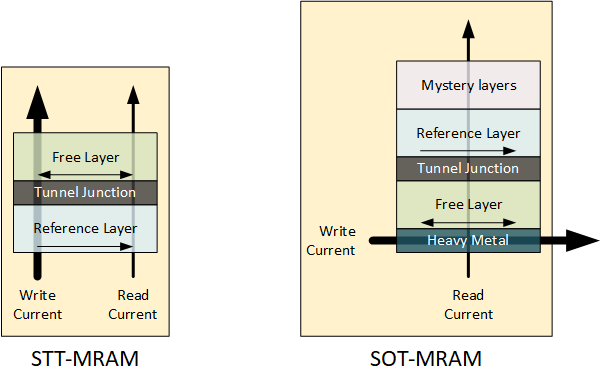
As a quick review, an STT-MRAM bit cell consists of a so-called pinned or reference layer, with a fixed magnetic polarization, at the bottom of the cell stack. It’s followed (moving up the stack) by a tunnel junction and then a so-called free layer whose magnetic direction can be set. This is a two-terminal device, with the terminals being at the top and bottom of the stack.
To write this cell means to set the direction of the free layer as either parallel or anti-parallel to the magnetic direction of the reference layer. The parallel direction allows more current to tunnel through, giving a read operation that looks for the amount of tunneling current to detect the state. The state is set by running a higher current through the cell; a read operation involves a lower current.
And herein lies the challenge: the write operation is but a stronger variant of the read operation. So when you do a read, there’s a chance that you could disturb the state and flip it. Normally, an error-correcting code (ECC) helps to fix such errors so that, in a complete system, you are able to figure out the correct data even in the presence of a low level of data noise.
But here’s where things get tricky: if you want to read data faster – say, to compete with SRAM – you have to run a higher read current, which can do more disturbing damage, and which might start to outrun the capabilities of the ECC. In order to challenge SRAM, you have to have access times that compete with SRAM. STT Technologies (the MRAM company we’ve talked to most recently) said that they target a 10-ns access time, whereas, if they’re targeting long-term NVM storage, they go more for 25-50 ns.
Such faster versions will have lower endurance – the number of times the cell can be written. Note that endurance might easily be confused with the other key memory reliability issue, data retention. But the latter refers to how long data will stick around in the cell if you do nothing to it; nothing to do (conceptually) with endurance (although they can interact).
So, commercially, this is where things are now. We saw STT’s PSC technology, which got them closer to the SRAM goal, but there was still a lingering data-retention complication (which we’ll come back to). PSC technology will still have the read-disturb issue because it’s still programmed using a current that runs through (that is, perpendicular to) the various layers
A New MRAM Approach
Enter SOT-MRAM. It’s very similar to STT-MRAM, with a few critical changes. First, the cell gets flipped upside down so that the free layer is on the bottom. Then, under the free layer, there is a layer of what is typically a heavy metal such as W (which Imec used), Ta, or Pt. This layer is where the programming happens.
Instead of running a current perpendicular to the layers, here the write current is run from side to side, so-called in-plane. Read, on the other hand, happens just as with STT-MRAM. So, unlike STT-MRAM, SOT-MRAM’s read current follow a completely different path from the write current and so doesn’t disturb the cell state. This greatly improves the endurance of the cell. This structure, therefore, is a three-terminal device: a read terminal, a write terminal, and a common terminal.
Breaking the Symmetry
You might wonder about those mystery layers that I allude to in the drawing on the SOT side. No, that’s not how Imec (or anyone else) refers to them. I put that there because I don’t know what they’re made of – and that’s intentional. But I do know why they’re there, according to Imec’s explanation.
The way SOT-MRAM works is that, when current flows along the heavy-metal layer, the current segregates. Current of one spin direction rises to the top of the layer; the opposite-spin electrons move to the bottom. The top-layer electrons coerce the free layer, or at least that portion of the free layer closest to the heavy-metal layer. But, because the free layer is very thin – around 12 Å – in practical fact, the entire layer is affected.
But there’s a symmetry here that gets in the way of writing both states. In order to break that symmetry, a small (less than 100 Oe) magnetic field is required. This has been one of the gotchas behind this technology: the need to provide a small external magnetic field.
However, part of Imec’s work involved them establishing that magnetic field with some of the extra layers on top – the mystery layers. This being a critical piece of know-how, it’s a set of details that they’re not eager to disclose to just anyone.
So, the upshot is that Imec has put together an SOT-MRAM bit cell that has high endurance and an incredibly fast read time: less than 1 ns and as fast as 210 ps.
Note, however, that this is the speed of the bit cell – you still have address decode times and such to take into account. Which brings us to an important distinction: a bit cell versus an entire memory chip.
That Data-Retention Question
So let’s come back to data retention. When we covered STT’s PSC technology, we found that the data retention was not infinite while power was applied, the way it is with SRAM. The idea here is that most SRAM data, because it involves rapidly changing information like cache contents, doesn’t need to hold data for particularly long.
Still, it felt to me like there was some chance that some long-standing piece of data might degrade with no one knowing – in a manner that wouldn’t happen with SRAM. They said that, were this a concern, a refresh capability – much simpler than DRAM refresh – could seal the deal with little silicon area penalty.
That said, when I talked with Imec, they said that, with power on, data retention should be infinite – just like with SRAM. That seemed to conflict with what STT had said. So I checked in with STT, both to get their thoughts on the whole SOT-MRAM technology thing and also to try to break the apparent data-retention disagreement.
With respect to their general reaction to SOT, they see this as an interesting new technology that has a long way to go before it’s proven as good-to-go for commercial volume production. They apparently have some irons in this fire as well, so they’re not talking smack about it.
But I found myself more challenged with the data-retention question, since now they also seemed to be agreeing that, with power on, retention should be infinite. That was unlike what I thought I heard in our prior conversation.
As with many such disagreements, it turns out that there’s a reason for it and that, in fact, both sides are right – from their perspectives. The thing we have to do is to distinguish the bit cell from the entire device – just like we have to do with the read access speed.
If the bit cell is powered on, then it should never lose state. But that consumes a lot of energy, and one of the benefits of MRAM against SRAM is much lower power. They get that lower power partly by powering off the bit cell when not writing – even though the overall memory device is powered on. In these recent conversations, I was talking to bit-cell folks, so their perspective is the bit cell, pure and simple.
In the prior conversation, I had been talking to folks with a perspective on the overall device. So it’s true both that the bit cell has infinite data retention when powered on and that the same cell does not have infinite retention when the device is powered on – as long as the bit cell is powered off while the device is on.
It’s not clear to me that SOT-MRAM technology solves this problem. If I find out otherwise, I’ll update this story.


What do you think the prospects are for SOT-MRAM?