


The upshot: Trained AI models have to be adapted for specific inference implementations. New inference hardware was presented at Hot Chips by Intel, Xilinx, and Nvidia, and Mipsology has yet another inference option.
This week we bring the natural follow-on to the machine-learning (ML) training piece of a couple of weeks ago: ML Inference. We talked about the overall process before; here we pick up with the implementation and inference phases in the image below (which we introduced last time, with this week’s focus indicated by the yellow highlight). 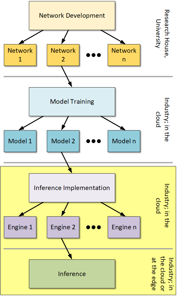
Implementing a Model
Having trained a model, we now need to make that model work on some sort of ML-inference hardware. Exactly what kind of hardware that might be would depend on where that model will be executed. In the cloud? Then probably you’ll use a beefy processor. At the edge? Probably not so much; a light touch is needed there.
The pure model doesn’t have anything to do with an underlying implementation, so it must be adapted in a few different ways.
First, many inference platforms – especially if targeted at the edge – work with integer parameters. However, a model is built with floating-point parameters. In this case, you then need to quantize the parameters – something that will naturally affect the model’s accuracy. There are many options – even binary representation.
Neural networks can also often be simplified at this point. You start with a pre-designed network for training, but, once trained, you may find that certain nodes have very little influence on the inference outcome. If that’s the case, you can prune away that node.
Pruning nodes does have an impact on accuracy, so it’s common to submit the modified model for retraining to regain some of the accuracy.
Depending on what hardware you’re considering, you might also be able to do some fusing. Textbook networks have layers of nodes. Fusing might mean simply collapsing two layers together for execution purposes. You’re not changing the network; you’re changing how it’s run, hopefully making execution more efficient. This tends to work better for hardware-oriented solutions than it does for software ones, since software implementations often simply assign nodes to a processor and have it run.
It is possible, however, to literally fuse some nodes in the network. There are cases where the resulting network is no longer the nice, clean set of layers of nodes, but more of a jumble. Such a network can be harder to update, and, if it departs too far, it may not be possible to reintroduce it to one of the major training frameworks for further training.
All of these efforts are done with a specific underlying inference engine in mind. The final step, simply called “inference” in the drawing above, is where the model is deployed in a system – at the edge or in the cloud – and it’s doing real work.
Alongside the training SoCs presented at this fall’s Hot Chips conference, a few inference-oriented SoCs were also presented. It’s reasonable to think that hardware for training and inference might really be pretty similar. They share the need to reduce the amount of data movement to and from memory, for instance. And multiply-accumulate (MAC) circuits still rule the day. But there are some differences:
- Training involves both forward and backward propagation of activations and weight corrections, respectively. Inference involves only the forward movement of activations.
- The performance requirements of training relate to how long it can take to train a model over a large set of labeled samples. The performance requirement for inference is the amount of time it takes to execute a model on a specific instance (image, frame, sentence, whatever).
- Training aims for a given level of accuracy, and it can continue until that accuracy is achieved in the “pure” model. Implementation may require some changes to maintain that accuracy. Once implemented, accuracy is no longer an issue for field inference; it’s baked into the deployed model (allowing for improvements via subsequent updates, if needed).
Inference Options
With all of that, then, as background, let’s look at three different architectures presented at Hot Chips – plus one more inference option. They’re all pretty much centered on providing lots of MAC access, with an attempt to ease data movement. Note that both weights and activations involve moving lots of data around. But weights are different in that they’re a fixed part of the model, and, if you had enough compute resources (no one does, so this is theoretical), you could put them into local memories and leave them there forever. Activations, on the other hand, are generated in real time for each inference, so there would always be some movement (short- or long-distance) involved with them, regardless of the architecture.
All of these have an accompanying software component both for adapting a raw model to the hardware and for real-time control.
I’ll be brief with each one, focusing on highlights. There’s so much more detail to get into if you wish to do so on your own.
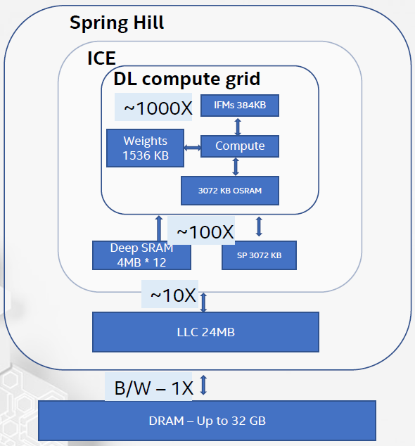
Intel’s Spring Hill
This is the inference side of their Nervana program (NNP-I); last time we saw their Spring Crest training side (NNP-T). Like most of these architectures, it’s hierarchical, with clusters of elements that contain computing kernels. At the top level, you have a collection of inference computing engines (ICEs) with coherent cache. Resources and performance are shown below.
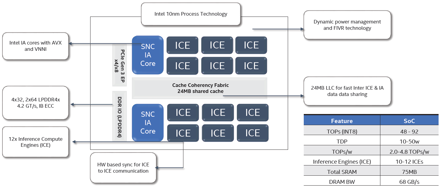
(Click to enlarge. Image courtesy Intel.)
The next level of hierarchy takes us into the ICE. It includes various types of memory and associated movement and management logic, a Cadence/Tensilica DSP for vector processing, and the deep-learning (DL) compute grid. Tasks can be allocated so as to minimize throughput or latency.
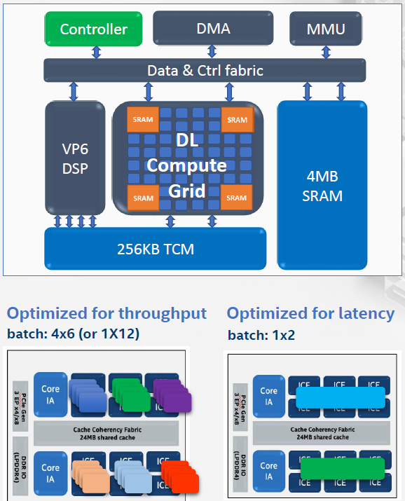
(Click to enlarge. Image courtesy Intel.)
The DL compute grid is an array of DL compute engines, shown below. Each of these has multiple compute elements. It also has post-processing capability fused in for such things as non-linearity (sigmoid, ReLU, etc.) and pooling.
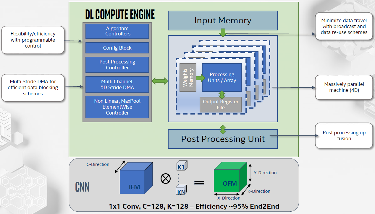
(Click to enlarge. Image courtesy Intel.)
They use various levels of caching to help with the memory-access burden, with each hierarchical level increasing bandwidth by roughly a factor of 10.
(Click to enlarge. Image courtesy Intel.)
They claim to process 3500 instances per second on a ResNet50 network, using 10 W of power. That’s 360 images/s/W, for an overall efficiency measure of 4.8 Tera-operations per second per watt (TOPS/W). Scaling from 2 to 12 AI cores results in a performance improvement of 5.85x.
Xilinx Versal AI Engine
[Editor’s note: because we received no response to our request to use their images, we’ve had to pull the images. I’ve tried to modify the text slightly to make up the difference, but you’ll need to somehow access the full presentation to get the full picture.]
Xilinx presented their Versal architecture. While I’m not going to address the entire thing, I will focus in on the AI engine that they have embedded. It’s distributed, with 400 tiles (133 INT8 TOPS peak), non-blocking interconnect (10 32-bit channels per column, 8 per row, 20-Tbps cross-sectional row bandwidth), and distributed memory blocks (12.5 MB L1, multi-bank shared with neighboring tiles, distributed DMA).
The computing tile consists of a scalar unite, a vector engine, address-generation units, instruction fetch and decode, and interfaces for memory and streaming. The vector engine includes scalar, fixed-point, and floating-point engines.
They focus a lot on their memory hierarchy, featuring two levels of cache (one of which we’ve seen). Part of that discussion involves the interconnect possibilities when loading L2 cache via a flexible crossbar switch. L2 contents can then be broadcast or multicast to L1 cache within the tiles.
Bandwidth and memory quantity across the hierarchy are: >64 GB DRAM moving to 16.3 MB of L2 SRAM at 102 GB/s, with L2 contents moving to L1 at 1.6 TB/s. The L1 cache consists of 128-kB 4-core clusters that can communicate at 38 TB/s.
They were able to run convolutions such that the vector processor operated at 95% of its theoretical performance. They also showed performance on GoogleNet3 and ResNet50 networks, comparing speed on this architecture to an equivalent implementation on their older Virtex UltraScale+ architecture (which doesn’t have a dedicated AI block). Those two networks were projected to run 7.2 and 5.8 times faster on the new architecture than they did on the old one.
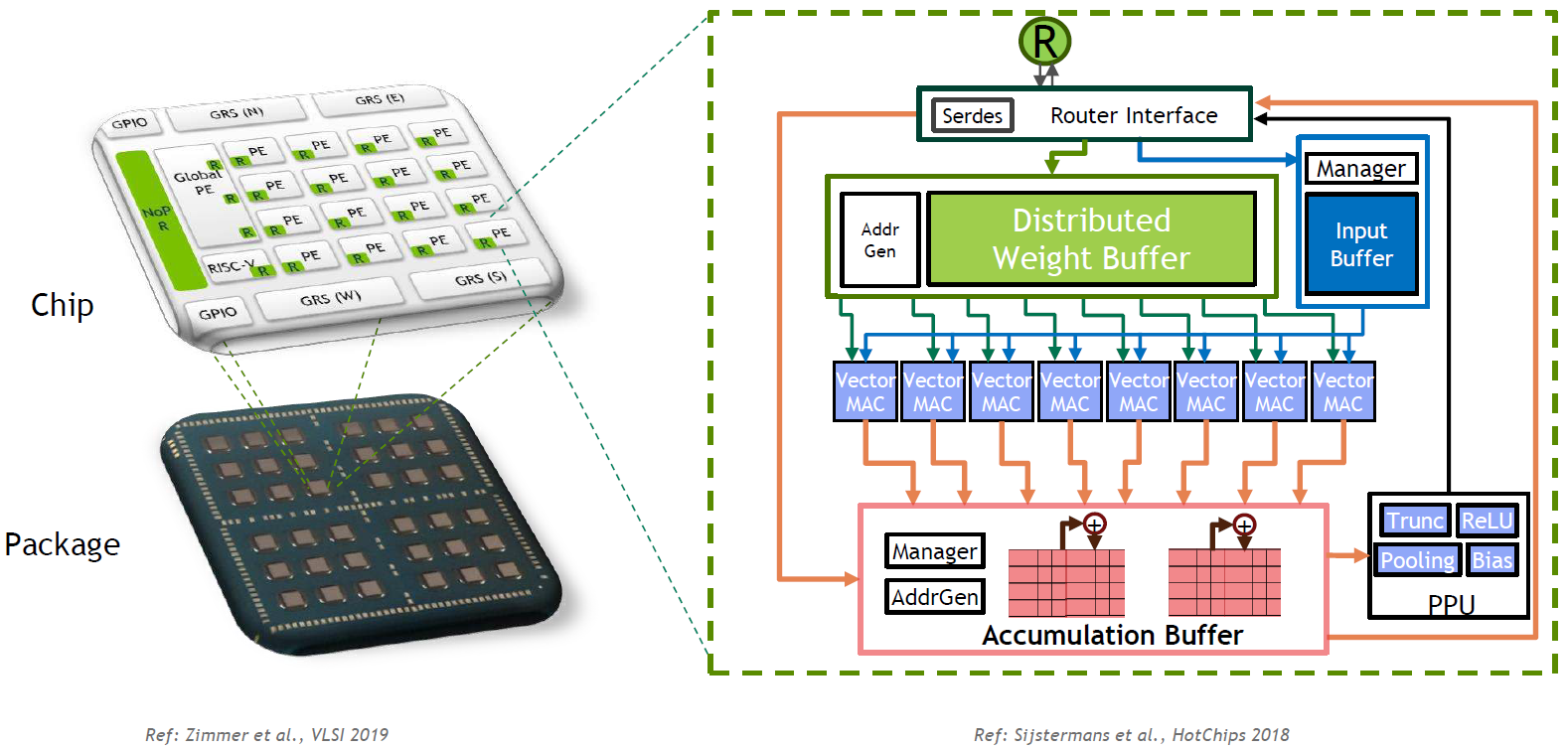
Nvidia MCM
Just as we focused on “how they did it” for the Cerebras technology in the earlier training article, here Nvidia has done an interesting implementation that itself deserves some discussion. In the never-ending question to populate as many computing resources as possible, they’ve got a multi-chip module (MCM) implementation. Note that, unlike some of the other projects we’ve seen, this is a research chip, and so it doesn’t have a brand or other marketingware associated with it.
We can see their entire hierarchy in the following image. Note that the highest level is the MCM, with 36 identical chips.
(Click to enlarge. Image courtesy Nvidia.)
The elements on the chip are interconnected using a network-on-chip (NoC); not a new notion. But that notion has been further leveraged to interconnect the chips on the MCM – something they call a network-on-package (NoP). The NoC is a 4×5 mesh using cut-through routing and capable of multicast. Latency is 10 ns/hop, and bandwidth is 70 Gbps/link (at 0.72 V power). The NoP is a 6×6 mesh with a router on each chip having four interfaces to the NoC. The routing is configurable so that you can route around bad links (or even chips). Latency is 20 ns/hop; bandwidth id 100 Gbps/link.
The compute engine is capable of 128 TOPS, or 1.5 TOPS/W.
(Image courtesy Nvidia.)
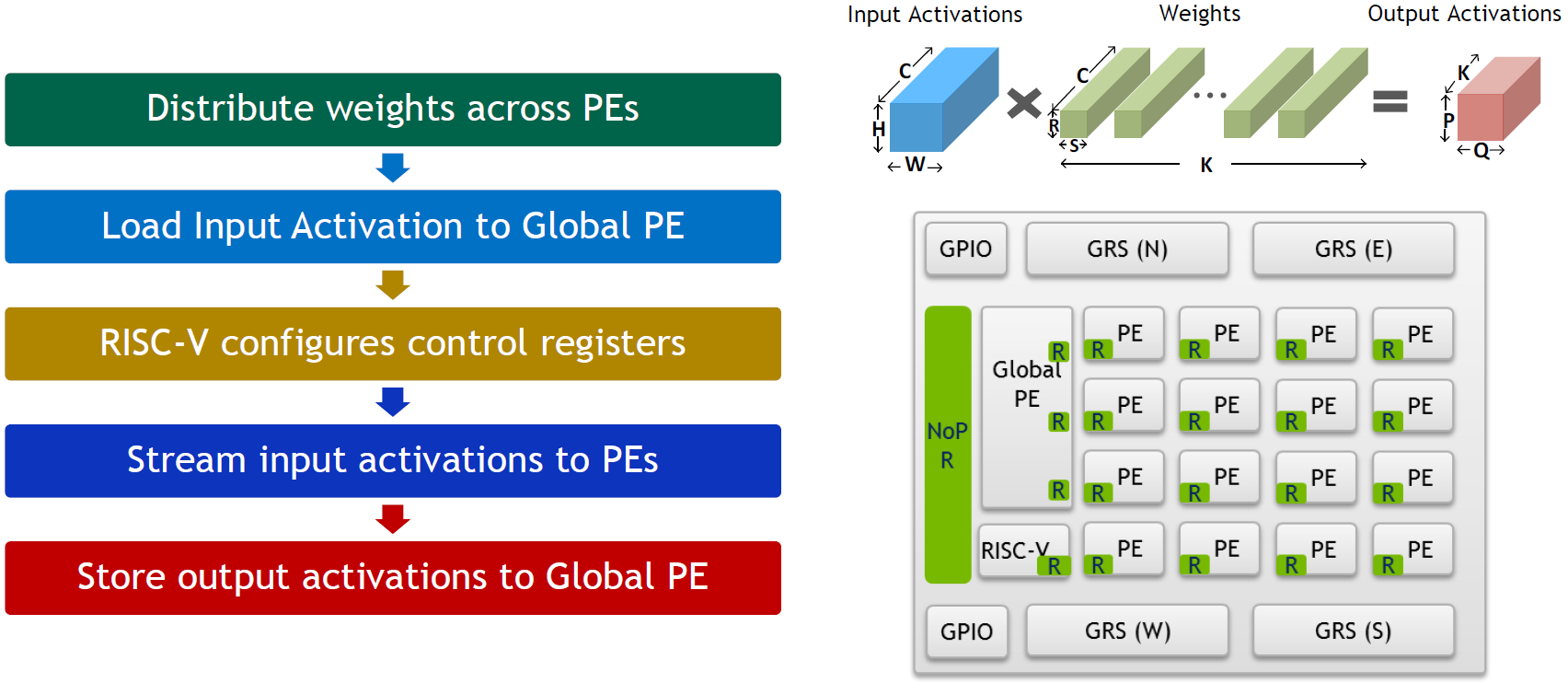
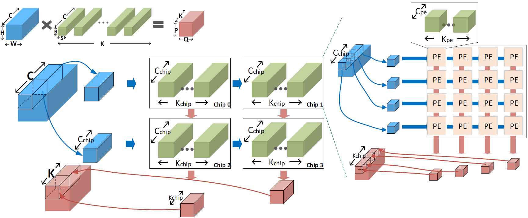
They provided more detail on how they implement a CNN in their architecture. Note that the activations enter and leave through the global PE before being distributed to or collected from the individual PEs.
(Click to enlarge. Image courtesy Nvidia.)
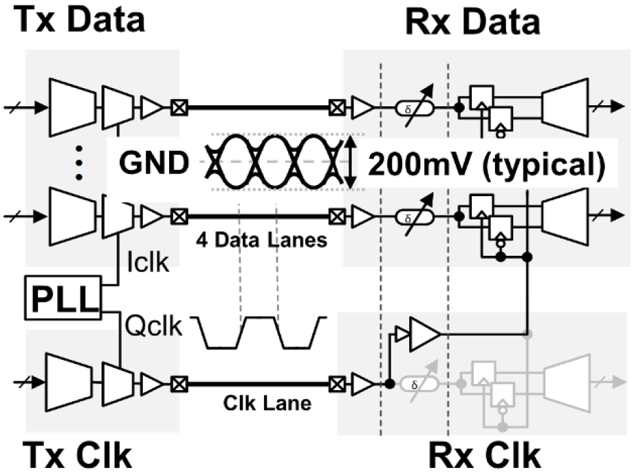
Now, you may be wondering, as I did at first, what this “GRS” thing is. Turns out it’s a different PHY for interconnecting the chips: ground-referenced signaling. Instead of using a signal that switches from ground to some level, with a reference voltage in between, it switches between a positive and a negative voltage, with ground in between – perhaps because ground is pretty much the most stable level you can get (almost by definition, since every other voltage is defined relative to ground). For those of us with a bit more… experience under out belts, it reminds me of the old ECL logic, where ground became the top rail because of its stability.
(Image courtesy Nvidia.)
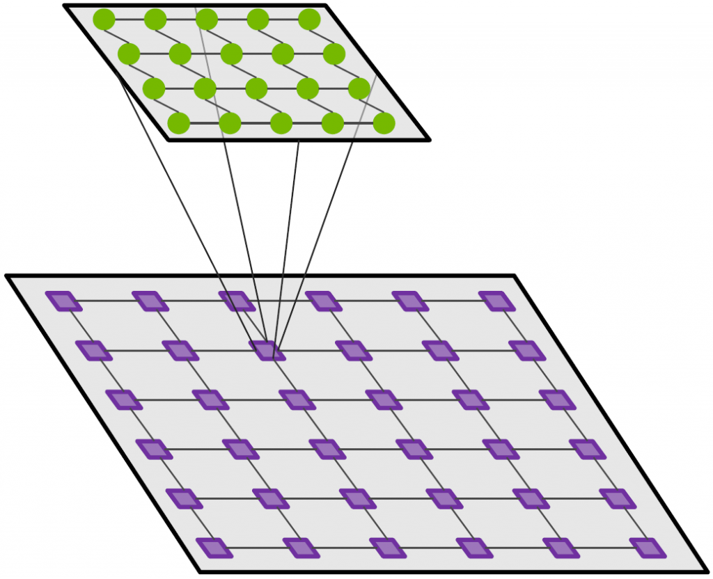
They also talked about how they partition up tensors for distribution throughout the overall hierarchy. This appears to be classic data partitioning, with different engines working on different parts of the tensor.
(Click to enlarge. Image courtesy Nvidia.)
They also spent some time discussing their design approach, which I won’t explore here in detail. But they said that, through extensive use of agile methodologies and logic reuse, they were able to design this whole thing in six months with fewer than 10 researchers. Dang…
Mipsology
Finally, we have a solution that I heard about outside of Hot Chips. And, in fact, this isn’t about leading-edge chips that might someday be available; it’s closer-in technology that’s available now.
Their idea is to use FPGA logic to be the inference engine, but to make it accessible to high-level data engineers who don’t know an FPGA from the FDIC. One common way to bury an FPGA is to use C++-to-DSL translation, but these higher-level (from an abstraction standpoint, not management) folks may speak only Python, not C++. Mipsology also doesn’t do the lego-together-predesigned-blocks thing. Instead, they have one FPGA image that’s used for all networks, and it consists of a variety of resources – multipliers, adders, memory, and such – that essentially provide a customizable sea-of-MACs. Any differences between networks and models are handled at higher layers in the software stack.
It’s built as a PCIe plug-in card, most likely for use in the cloud – or somewhere where the price point can support an FPGA=based module. The full stack is shown below.
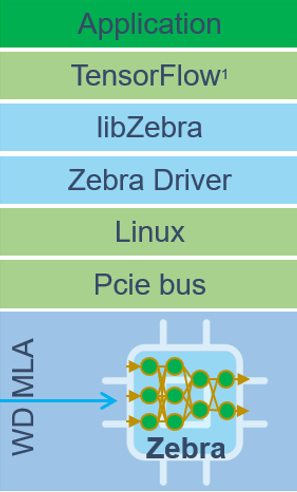
(Image courtesy Mipsology.)
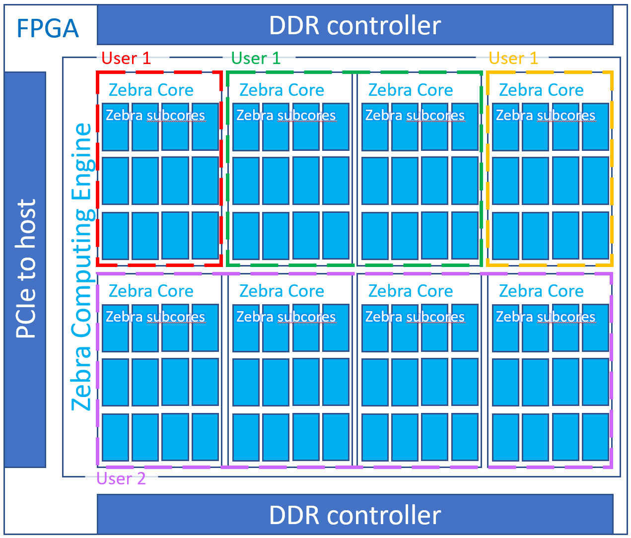
They allow allocation of resources between one or more networks running at the same time – useful for a cloud-based resource that may be shared. It’s scalable such that they can maximize parallelism where the resources are available (tracking dependencies as needed) and serialize when they can’t go parallel.
(Click to enlarge. Image courtesy Mipsology.)
They’ve also designed it to look pretty much like a GPU board that the cloud guys are already used to working with. Under the assumption that training is most likely to be done with GPUs, they try to minimize the amount of work required to adapt to the FPGA approach, as indicated in the following figure. Or, for applications already doing inference on GPUs, the transition involves only a change in a Linux command.
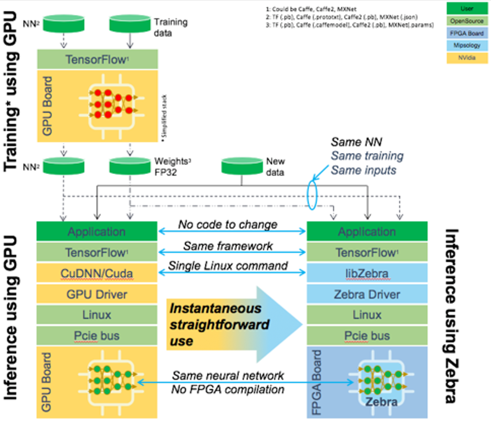
(Click to enlarge. Image courtesy Mipsology.)
And that ends our brief run-through of inference options. There is more to come in our discussion of AI technologies, because lots of new things are on the way. Stay tuned.
More info:
Nvidia: being a research project, there is no web page dedicated to the architecture they presented. You can access it in the Hot Chips proceedings.
Sourcing credit:
Robert Lara, Sr. Director Marketing & Business Development, Mipsology
(The remainder are from Hot Chips presenters)


What do you think of the current Mipsology and the future SoC ML inference approaches?