


Machine-learning (ML) training is a beast of a problem. And it would appear that the industry is unleashing silicon beasts in order to battle that training beast. Some of those were revealed at the recent Hot Chips conference, including the biggest “chip” ever made. In honor of the benefits of being large, this article will be longer than average – and still leave things out. It’s a beast of a topic!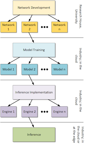
Most of what I’ve covered in the past has been about machine-learning inference. For anyone newly wading into this space, machine learning has two phases. In the first phase, a model is trained; in the second phase, that model is deployed for its intended application – inferring something about real-world input in accordance with the training. It can also be helpful to split training into two: generic training and then model implementation on a specific inference platform.
ML: The Big Picture
In fact, there’s an earlier phase that we talk even less about: the creation of a neural-net architecture. As far as I can tell, that’s a job for research houses and universities. As an average engineer, you don’t just wake up one day and decide to invent a new neural network by the end of the day. There are a number of networks out there being deployed, but it’s few enough to where they have names – like ResNET or Google’s BERT network (or further attempts to do better than BERT – ERNIE at Baidu (cute!) and RoBERTa at Facebook).
Each of these networks is intended for a general task – natural-language processing in the case of the BERT (& co.) networks. But they have to be trained for the specific tasks for which they might be used. That might be understanding voice commands from a specific smart speaker or comprehending legal documents.
The training process brings another couple of common terms, again, for anyone new to this. You’ll hear a lot about “parameters.” I’ve heard this term defined both as “weights and activations” and as “weights.” A model has only weights, since the activations are calculated in real time during inference. So the activations aren’t built into the model the way the weights are. So using “parameters” as a synonym for “weights” feels more appropriate to me, since they’re a static property of a trained model.
You’ll also hear about “hyperparameters.” It turns out that some (but not all) networks have settings that you can apply before training starts. If we were talking about silicon IP, we’d probably simply refer to those settings as “parameters.” But that would cause confusion with the other parameters – the ones we’re trying to train. So instead, we call them hyperparameters.
Once we’re done training, we need to adapt the trained model to a specific computing platform, which I’ve indicated as a separate phase in the image above. That gives us four distinct phases, of which we’re going to focus on the second: basic training. (We’ll follow up with more inference in a few weeks.)
ML Training
You know, we look at generic “here’s-what-they-are” neural-network drawings, and we see a few nodes in each layer, with a few layers making up the model. That makes a drawing and visualization more manageable, but let’s not kid ourselves: these things are giant. An overall model may have billions of weights. And each of those weights has to be calculated – or, more accurately, adjusted – with each training sample. Newcomer Cerebras describes this as peta- or exascale computing. It proceeds something like the following:
- Start with a chosen network, which will have default weights set.
- Run a sample through it. The sample will be labeled, meaning that we know what the engine should infer. The calculated activations propagate forward through the network to see what the network actually infers.
- If the outcome is correct, then great. But, most often (at least, early in the process), it won’t be, and so you need to figure out how far off it is and make a correction at the last layer. Then that correction implies corrections in the prior layer, and so forth – propagating backwards through the network to tweak all of the default weights.
- This happens for each sample – millions of samples, potentially – and, for each sample that doesn’t infer as per the labeled expectation, more adjustments are made until you reach your desired accuracy level.
- That accuracy level is determined by running a set of test samples that weren’t part of the training. That’s the true test.
So how does this happen in real life?? After all, it’s being done today – although perhaps not at the bleeding billion-parameter edge. But still, it’s a ton of computing. And, it’s mostly being done brute-force – lots of FLOPs (since this is primarily a floating-point process). But then there’s this issue of moving all of the weights around – as well as the activations being generated for each sample. And that’s a huge problem. You hear talk of “hitting the memory wall” – where your performance is determined not by the calculations, but by the time it takes to move the data around. We’ve seen this for inference, and it’s even more important for training.
There are a couple of fundamental ways of tackling this. One is data parallel – you replicate the same model in a ton of different machines, running different samples through the different versions and merging the results at the end. The other is model parallel – you split the model up and do the training on a portion of the model, with different machines working on a different portion. At the end, you stitch the thing back together.
With a data-parallel approach, each machine or cluster performs a number of data reductions, reducing the amount of machine-to-machine communication. With model parallelism, however, because a single model is distributed – say, layer by layer, or even node by node – much more communication – and therefore much higher bandwidth – is required.
This has raised a couple of different things to pay attention to in new training SoCs: the amount of computing that can be done on a single die, often involving discussions of granularity, and the ease with which one can gang together multiple instances of the chip – so-called scaling out. The latter gets to how the training acceleration boards are built, with multiple chips working together to solve the problem together.
Measuring Performance
New architectures are being proposed that better balance the computing and bandwidth needs of the problem. And even newer ideas – like the inchoate in-memory computing notion – are being worked to tackle this challenge (although we’ll defer that discussion until later). We’ll look at some of the new architectures in a moment, but, before we do so, how can we ever evaluate which of these is the best?
Right now, it’s up to individual companies to share their results – and you may or may not be able to compare the results of different companies if they’re using different measures. Some are higher-level – like the announcement that Nvidia made during the Hot Chips conference. They touted their results for the BERT network, training it in under an hour – and performing inference in just over 2 ms.
But, to get more specific and still ensure comparability, you need benchmarks, and there is a group – MLperf – that is tasked with doing just that. They’ve completed their job for training; inference is still a work in progress. We’ll dive into this topic at a later date, but some of the news surrounding the Hot Chips conference was based on results to date.
New Hardware for a New Problem
With that then, let’s look at a couple of the architectures that were presented at Hot Chips. Two are from well-established companies (to say the least); the other two are from newcomers, reflecting the incredible number of startups trying to be the next big thing in AI architectures. We could delve into incredible detail on each of these; we don’t have space for that, so this will remain somewhat high level.
Intel Spring Crest
This SoC is part of Intel’s Nervana program. It’s a neural-network processor for training (or, as they call it, NNP-T). Their goals are succinctly stated on one of their Hot Chips slides:
- “Train a network as fast as possible within a given power budget, targeting larger models and datasets
- Balance between Compute, Communication, & Memory
- Re-use on-die data as much as possible
- Optimize for batched workloads
- Built-in scale-out support
- Support future workloads”
It has around 27 billion transistors, with lots of focus on close access to fast memory and fast I/O. The high-level architecture looks as follows (where TPC stands for Tensor-Processing Cluster).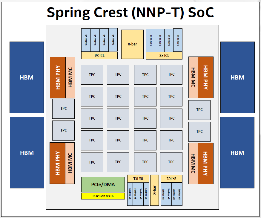
(Click to enlarge. Image courtesy Intel)
As you’ll see with the next image detailing the TPC, in addition to the high-level connections to HBM memory, they keep local memory around to help reduce the need to move data into and out of the HBM memory. They obviously have multiply-accumulate (MAC) logic, but they also have a dedicated convolution engine for CNNs. Uniquely amongst the architectures we’re discussing today, they make use of the bfloat numeric type, which maintains the range of a longer number while sacrificing precision. And, of course, there’s the interconnect, which enables scale-out.
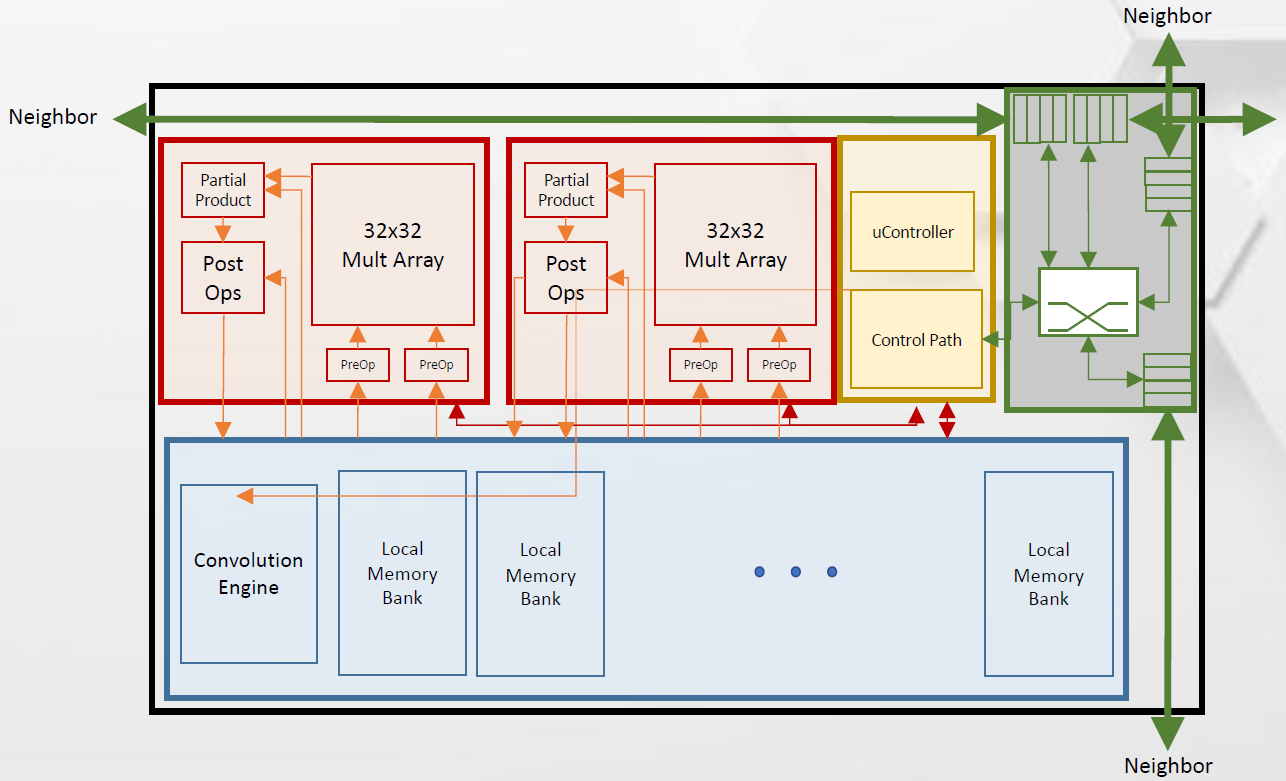
(Click to enlarge. Image courtesy Intel)
They have a limited tensor-based instruction set and a programming model that supports distributed programming, whether within the chip or across multiple chips. It would appear to be targeted at specialist programmers, not your garden-variety developer, with explicit software memory management, message passing, and synchronization primitives.
Huawei
Huawei’s DaVinci architecture (branded as Ascend for training chips) takes a different approach to resource balancing. It has scalar (1D), vector (2D) and matrix (3D) units that are shared. C-like programming allows developers to access these resources between multiple hardware threads. They claim performance more than twice that of Google’s Tensor Processing Unit (TPU).
The basic core is configured into a 16x16x16 cube**. Like Spring Crest, this architecture also leverages HBM stacks collocated on an interposer with the main SoC.
They’ve done lots of work to take a complex parallel multi-threaded architecture and make it easier to program by developers that are more comfortable with sequential code (as most of us are).
The DaVinci core is about more than training. In addition to featuring in their Ascend training SoCs, they also have a mobile application processor, automotive, ML inference and wireless SoCs (or, at the very least, they have drawings of them).
Habana
Habana sees themselves as having the opportunity to leverage the benefit of what’s been learned through the use of GPUs – without the legacy of graphic rendering. So they were able to start from scratch. They have their own TPC – this one standing for Tensor-Processing Core. I haven’t seen a drawing detailing the contents, but they describe it as a C-programmable VLIW SIMD engine with local memory. Per their whitepaper, it’s been optimized for:
- “GEMM [General matrix multiply] operation acceleration
- Tensor addressing
- Latency hiding capabilities
- Random number generation
- Advanced implementation of Special Functions”
The Gaudi chip, which uses the TPC for training (as contrasted with the Goya chip, which uses it for inference) uses an eight-TPC cluster as shown below.
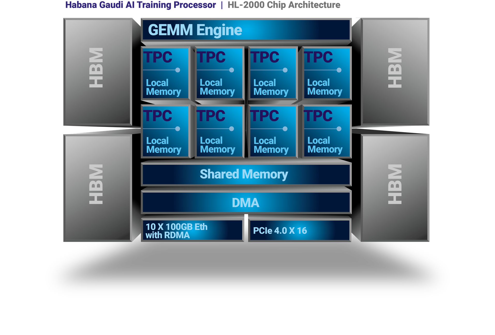
(Click to enlarge. Image courtesy Habana.)
They have a couple of big claims to fame. One is their means of scaling out. They use PCIe to talk to the host only. For scaling out to other Gaudi chips, they use RoCE – RDMA over Converged Ethernet. Essentially, it’s Infiniband’s RDMA capability tunneling through Ethernet. This makes data-center interconnection much easier, since it relies on standard Ethernet rather than on a proprietary connection. Each Gaudi chip has 10 100-Gb/s Ethernet channels.
In their HLS-1 board, which combines eight Gaudi chips, seven of the Ethernet channels on each chip are used to talk to the other seven chips for non-blocking all-to-all connectivity. The remaining three are available for external scale-out. Scaling to multiple boards is possible with a standard Ethernet switch.
The other advantage they tout is software-oriented: It’s straightforward to port over existing code from, e.g., a predictive analytics application, and create custom Gaudi kernels that maintain the accuracy of the original.
Cerebras
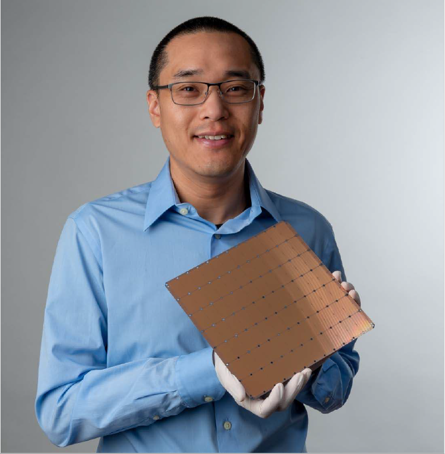
Finally, we come to what is, if nothing else, the most startling chip in the bunch. If you can call it a chip, that is. Cerebras effectively squared the circle*, taking the largest square that could be placed inside a wafer and calling that their chip. They had one at the conference, making it more than vaporware.
(Image courtesy Cerebras.)
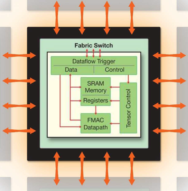
I’m not going to focus so much on the architecture here as much as on how the dang thing was built. Obviously, they can’t image the entire chip using a single reticle exposure. Fundamentally, they still have to act as if the wafer is populated with an array of dice. So what they do is make all of those “dice” the same and then connect them together… somehow. They worked closely with TSMC on that last bit, and I couldn’t pry any more information out of them; they consider it secret sauce. They did say that they didn’t take an “obvious” approach. The basic tile looks like the following:
(Click to enlarge. Image courtesy Cerebras)
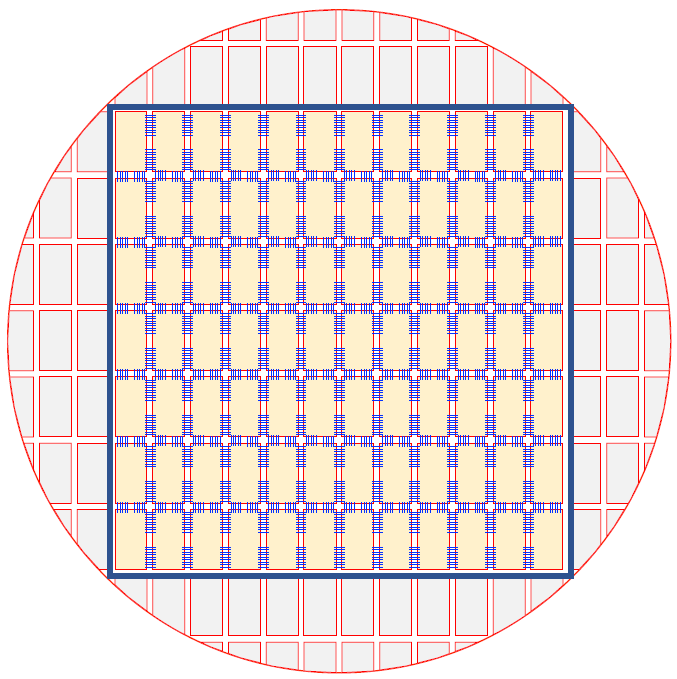
As indicated here and in the wafer-level image below, they have a way of interconnecting those tiles across the scribe lines, which still exist. So, somehow, they expose the entire wafer just like any other wafer, and then they add those interconnections.
(Image courtesy Cerebras)
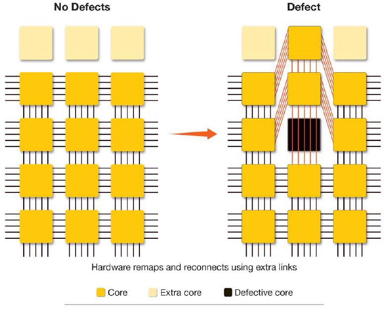
Of course, the obvious question at this point would be, what good is a die that has 0% yield? After all, your typical wafer might yield in the 90% range for some particular chip, but it has to be 100% – and no less – to get one of these beasts to yield. So they use the obvious solution when problems like this arise: redundancy. They can route around faulty circuits as shown below.
(Image courtesy Cerebras)
The “die” size creates a number of other problems. Like, how the heck to you attach this to a PC board? After all, you’ve got a “chip” the size of a board that will have a thermal response different from that of the board. How do you keep it connected? They’ve devised a custom connector to absorb the difference between the coefficients of thermal expansion (CTE) of the two materials.
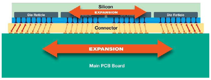
(Click to enlarge. Image courtesy Cerebras)
Next, packaging requires some precise alignment of a cold plate, the wafer, the connector, and the PCB. So they developed custom assembly tools and processes.
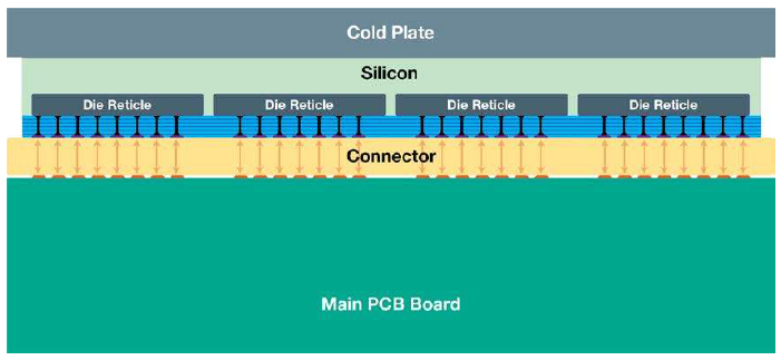
(Click to enlarge. Image courtesy Cerebras)
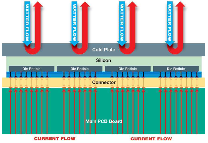
Finally, they had to figure out how to get power in and heat out. The edges of the die are so far from the center that typical approaches wouldn’t work. Instead, they use distributed cold-water flow, as well as distributed power delivery, so that power and heat come in and leave across the die, not through just a few places.
(Click to enlarge. Image courtesy Cerebras)
They’ve used TSMC’s 16-nm process, resulting in a die size of 46,225 mm2 containing 1.2 TRILLION transistors, 18 GB of on-chip memory, 9 PB/s of memory bandwidth, and 9 Pb/s of fabric bandwidth. And they say that it’s working.
If that doesn’t convince you that ML training is a beast, then nothing will!
*For literalists, no, they didn’t crack the classic construction problem, which is impossible. The square area isn’t the same as the circle area. And they didn’t restrict themselves to the rules of construction.
** I was unable to include figures for the Huawei DaVinci architecture, since requests for permission to use them received no response.
More info:
Sourcing credit:
Paresh Kharya, Dir. Product Mgmt and Marketing, Nvidia
Eitan Medina, Chief Business Officer, Habana
(The remainder are from Hot Chips presenters)


What do you think of the various machine-learning training SoCs presented at Hot Chips?