


We’ve looked at a lot of different solutions for AI computing, each trying to be somewhat more efficient than some prior architecture. However, pretty much everything I’ve been exposed to up until recently has reflected serious attempts to make calculations using CPUs, GPUs, and DSPs more efficient. Each of these has been some version of a von Neumann architecture, meaning you have someplace where you store all your data, and you then fetch that data when needed in a single-stream processing flow (with allowances for SIMD) through some processing unit (one of the three above).
But here’s the thing: for each synapse, you have to go out and fetch activations and weights out of memory, and then you have to multiply them and store the results before moving on to a new synapse. All that data movement is a serious consumer of energy – as is the multiplication. As if that weren’t bad enough, some of those circuits – multipliers in particular – chew up a goodly chunk of territory. And data movement takes time.
All of this might not feel so bad if it were all to happen in the cloud, as it mostly is today. But, as we’ve seen, there are serious efforts to move inference to the edge of the IoT network. Training is more computationally intensive, so it may remain in the cloud, but, once the neural net has been trained, then it can be imported into devices at the edge that will perform the inference task – which is really what the end application is all about.
At the IEDM conference this last December, there were a couple of particularly interesting papers that appeared to show some significant improvements in efficiency and power – as much as 3 orders of magnitude less energy consumption. There are a number of components that go into the improvements, so we’re going to walk through them to put the puzzles together.
Bye Bye von Neumann
The first change isn’t unique to these papers. There’s a serious effort afoot to move away from traditional architectures and implement what’s called in-memory computing, or iMC. The idea is that, rather than having one memory off to the side that acts as a dumping ground for all the different numbers that will be used, multiple memories are used. Each synapse becomes its own memory, and the computation happens locally. There’s no more of that costly data movement.
Of course, that means we need efficient, small memories and computing elements, so that’s a primary focus. We also need a way to compare these different architectures, so, before we dig in, let’s review some basic ways we can judge the best performance. Speed and power are obvious; we use our standard units of time and either power or energy. But how do we know if we’re comparing apples to apples? Having a faster or lower-power circuit may not count if that circuit does a lousy job of inference.
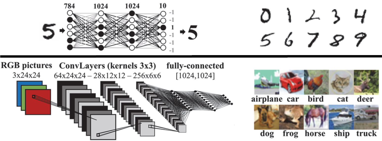
Comparing the effectiveness of different engines is gauged by measuring how well each engine can recognize something. This is often a vision task – as will be the comparisons we make below – but it could also be recognition of, for example, spoken natural language.
For vision, there appear to be two basic databases that are often referenced. Indeed, in the two papers we’ll discuss, they both refer to these two databases. This commonality provides a better way to benchmark results. The two databases are:
- MNIST, a large collection of handwritten digits
- CIFAR-10, a large collection of images
We’ll refer to these when we discuss results. As a baseline, one of the papers quotes a pure software approach (von Neumann) as achieving 98% recognition of digits in the MNIST collection. Can these new hardware approaches get there – or even exceed that? Let’s explore.
RRAM for iMC
Resistive RAM, or RRAM, is frequently mentioned as a candidate for the memory that would implement a synapse. It’s a non-volatile memory, but there are variants on how it’s implemented. The thing is, at least at present, it remains a relatively unreliable memory due to variation and asymmetries when programming different states. This is a common theme for both papers, but it’s addressed very differently in the two approaches. So much so that the second paper we’ll look at involves an alternative to RRAM.
But let’s stick with RRAM for the moment. It’s used in an architecture developed by a team from Aix Marseille Univ, Univ. Paris-Sud, and CEA-LETI, all in France, members of which I was able to talk to at IEDM. Their story is about both robustness and power. Let’s start with the effort to make things more robust.
The way that RRAM variability is typically handled is by implementing error-correcting codes (ECC). Such circuits, by this team’s estimation, can cost hundreds to thousands of gates. That might not be a problem for a single, large memory, but here we’re talking about hundreds of synapses, meaning hundreds of memories, each of them needing their own ECC capability. Clearly a potential cost issue.
They came up with two solutions to improve robustness: a (mostly) novel memory cell and their approach to the neural net. I say “mostly” novel because they say that their type of cell has been implemented before, but no one has characterized the resulting robustness until this project.
They developed a differential RRAM bit cell. While the more typical version uses one transistor and one resistor for each cell (so-called 1T1R), they used a differential approach, meaning a 2T2R cell. Yeah, you might think that this makes the array larger – and, presumably, it does – but if it means you can get rid of ECC, that could be a good tradeoff. The figure below shows both the cell and the pre-charge sense-amp (PCSA) circuit used to read the memory.
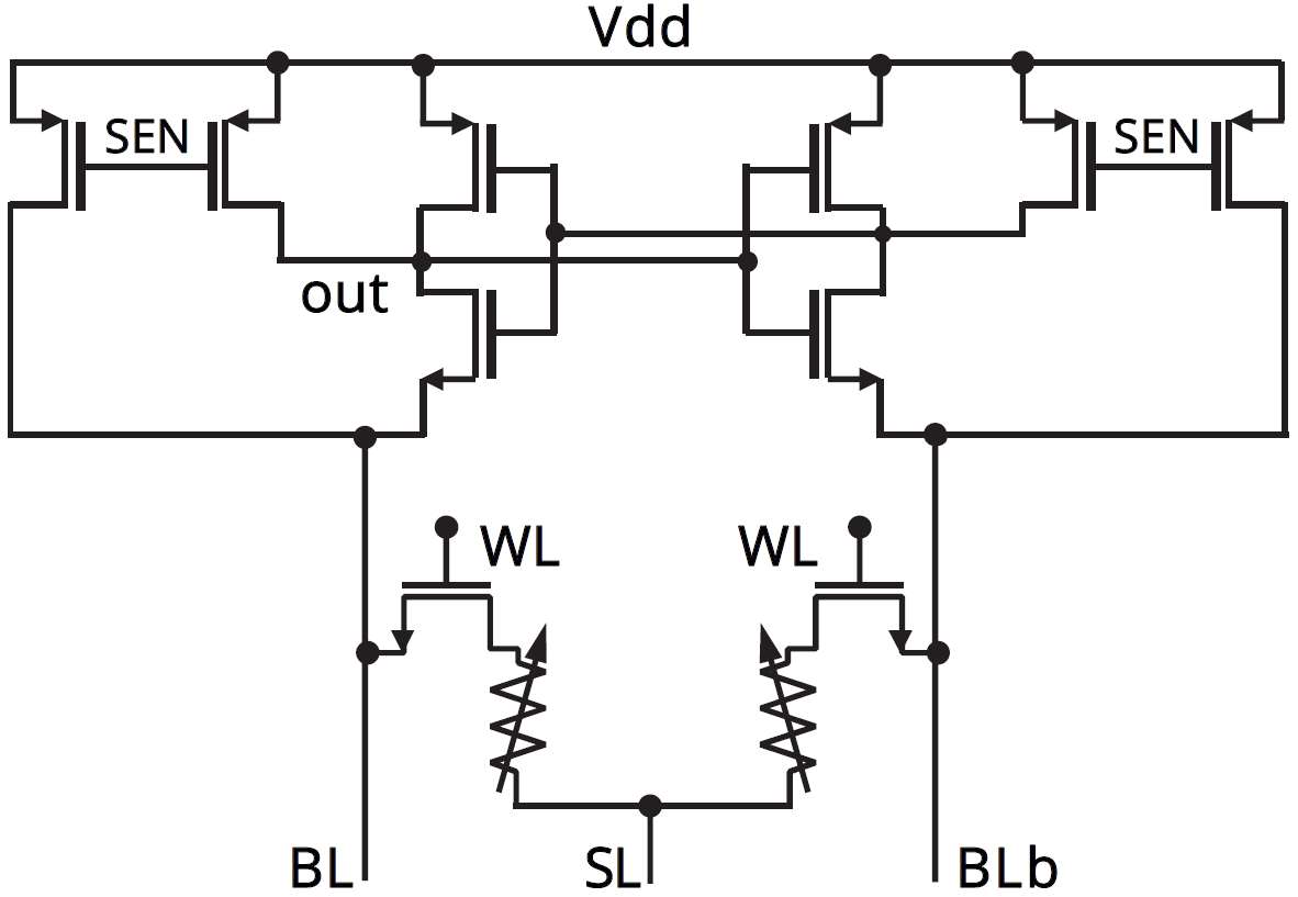
(Image courtesy IEDM. Image credit research team.)
Of course, one sense amp serves many cells, so only the transistor pair and resistor pair are the actual bit cell. The entire array, including peripheral circuits, is shown below.
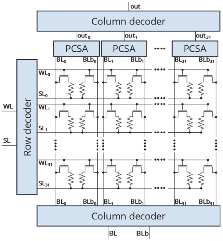
(Image courtesy IEDM. Image credit research team.)
The bit cell is built atop metal 4, using a stack composed of TiN/HfO2/Ti/TiN. The critical HfO2 and Ti layers are each 10 nm thick.
A bit cell of any memory technology is only as good as the ability to distinguish a 1 from a 0. Ideally, you want a wide gap between whatever reading (voltage, current, etc.) means a 1 and whatever reading means a 0. With RRAM, they’ve found that this gap decreases with use and aging, which limits the life of the memory. Now, if the memory starts to fail after a million years of use, who cares? Unfortunately, that’s not the case here, and endurance – that is, the number of write cycles before the memory becomes unusable – is an important characteristic
By using the differential approach, they’ve increased the endurance far beyond what’s possible with the more traditional 1T1R bit cell. That’s because you’re no longer looking at the absolute value of the bit value; you’re looking at the difference between two values, and that holds up longer.
So the bit cell is one way of increasing robustness. But they have another approach that overlays this one: going to a binary neural net, or BNN. In theory, this looks like any other neural net, except that, with most practical networks in use today, weights and activations are trained as real numbers and then discretized into integers for the final inference model. With a BNN, weights and activations can be either 1 or 0. From a practical standpoint, such networks take more work to train, since common platforms like TensorFlow and Caffe aren’t set up to do that – you have to fake it out, so to speak. But, in the end, it’s doable.
Going binary has two immense advantages:
- Multiplication reduces to XNOR.
- Addition reduces to so-called popcount, short for “population count,” meaning the number of 1s in a number, also known as the Hamming count. The team says that it takes something like seven gates.
So you lose an immense amount of circuitry, much of which chews up a lot of energy in the course of doing its job. Traditional CPU/GPU approaches, according to the team, consume in the micro- to millijoule range. Their approach is more on the order of 20 nJ for roughly the same performance (maybe just a tad better).
In addition, the XNOR gate can be implemented in the sense amp, meaning that a readout can already include the multiplication result. This is shown in the figure below. Of course, there’s nothing to stop someone from using a separate XNOR gate; it’s still way, way simpler than a multiplier.
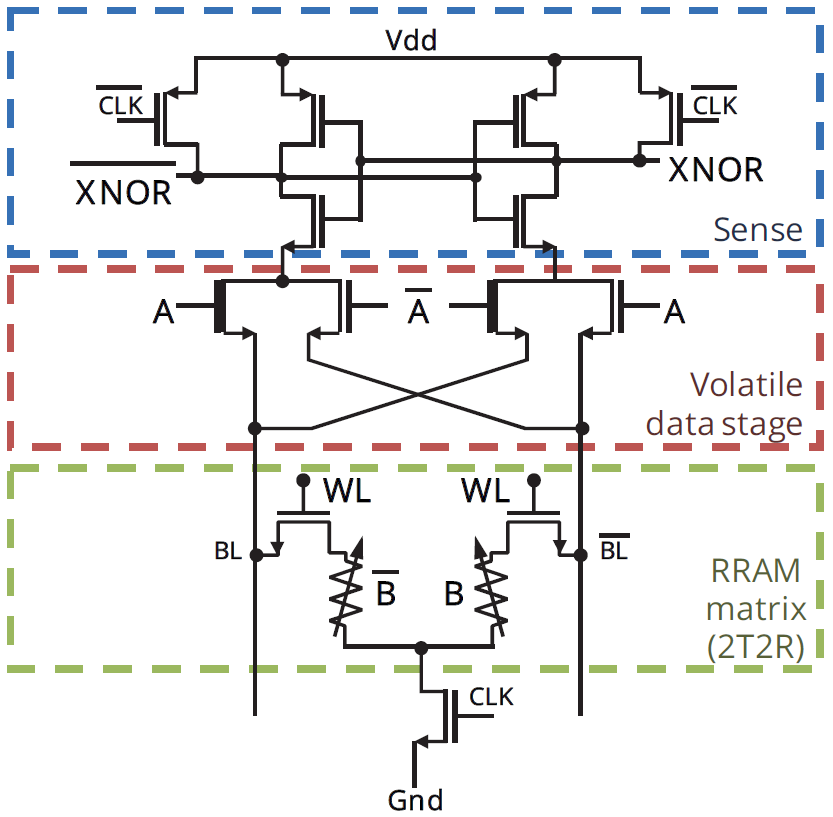
(Image courtesy IEDM. Image credit research team.)
So their final array looks as follows:
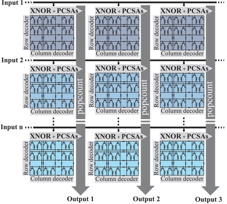
(Image courtesy IEDM. Image credit research team.)
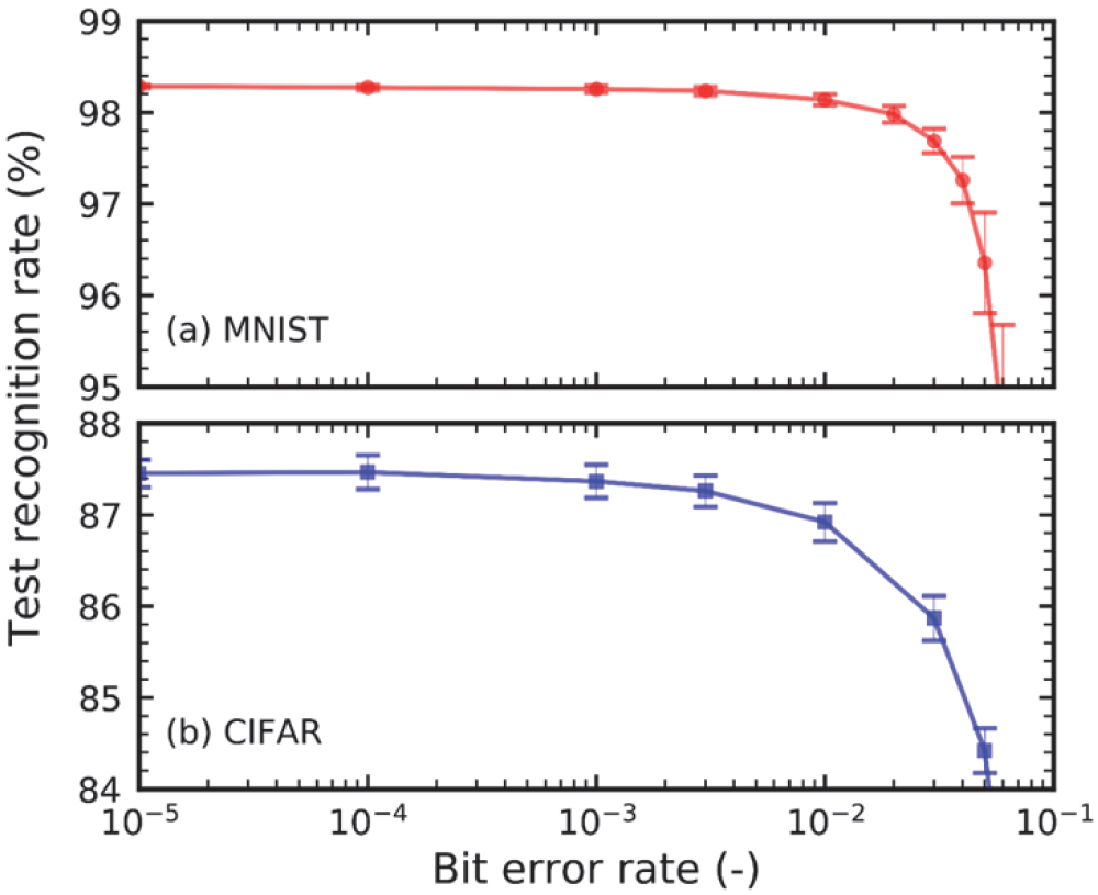
They tested their implementation against the MNIST and CIFAR-10 collections with two different networks, as shown below.
(Image adapted; courtesy IEDM. Image credit research team.)
On the first set, they achieved a recognition rate of 98.4%; on the second, they achieved 87%. More interestingly, however, was the fact that this approach appears to be error-tolerant. As they note, with most digital calculations, an error is catastrophic. And yet, they found that they could withstand an error rate up to 2×10⁻³ without significantly affecting the results. And they determined that endurance would extend into the billions of cycles.
(Image courtesy IEDM. Image credit research team.)
Going Analog
Meanwhile, another team from Arizona State, Notre Dame, and Georgia Tech went down the analog memory route. Problem is, RRAMs – at least of the sort that they were looking at – didn’t look promising. There are a couple of approaches to RRAM – one that leverages filaments and another that uses oxygen vacancies or charge carriers, referred to as filamentary and interfacial, respectively. They noted that filamentary memories achieved MNIST recognition of only 41%. Interfacial did better, at 73%, but required very slow programming since vacancies didn’t migrate very quickly.
Instead, they turned to a different cell, one relying on ferroelectric FETs, or FeFETs, for storage. These FETs replace the traditional gate dielectric with a ferroelectric material. Such a substance can have dipoles established in accordance with an electric field applied during programming. Most traditionally, this establishes a 1/0 binary cell, but partial polarization is now seen to be possible, so this provides the basis for an analog memory.
With such an array, they were able to get up to 90% MNIST recognition, but it required complex timing during the programming, resulting in a very large extra peripheral circuit.
To address this, they took advantage of a key observation: training must be done with higher resolution (> 6 bits) than inference, which can get away with less than 2 bits. One way of looking at this is that you train with a full-resolution number, which has, of course, MSBs and LSBs. For inference, you can do without the LSBs – in effect, rounding off the numbers.
So they used this information to create a cell that is a hybrid of volatile and non-volatile storage. The LSBs are volatile and are eventually dropped; the MSBs are non-volatile, implemented through polarization of the FeFET. They call the cell a 2T1F cell, and it looks as follows. The ferroelectric material used was Hf0.5Zr0.5O2.
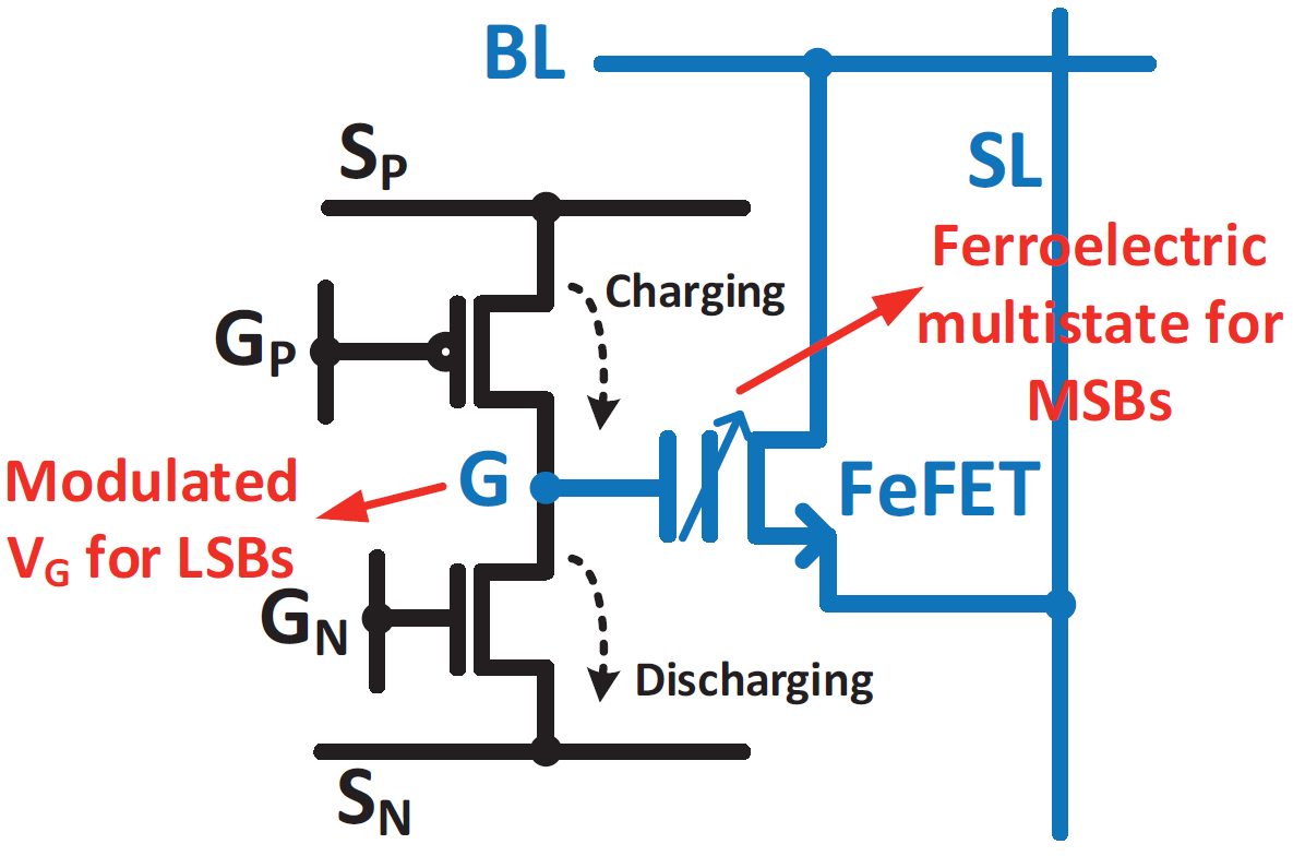
(Image courtesy IEDM. Image credit research team.)
That G node is the key: its value is set by pulses applied on GP to charge it up and on GN to discharge it. During the training phase, these pulses are applied to adjust the value and, in theory, once training is complete, it can be loaded into the FeFET – with lower resolution. But there’s a real-world catch: that G node leaks, and in a matter of a millisecond or so, it can lose the equivalent of a pulse.
So, instead, periodically during the training, they go ahead and load the FeFET, even though they’re not done. They then reset the G value to the middle of its range and continue on. Apparently, this reset value isn’t the ideally best value, but the circuit required to optimize the value is large, so this is “good enough.”
With this, they were able to achieve recognition rates of 97.3% on MNIST using a 6-bit training/2-bit inference implementation and 88% on CIFAR-10 with 7 bits/2 bits.
It also occurs to me that these two papers could almost be used together, since the second one involves training – not something currently being proposed for the edge. (Given current training approaches, it doesn’t even make sense to do at the edge.) So this second paper could be used in the cloud for training, and the first paper could handle the inference in the edge. The “almost” reflects one big gotcha: the training doesn’t create a BNN. Perhaps there’s more work that could integrate these approaches.
You can find all the gory details for both of these approaches in their respective papers.
More info:
“In-Memory and Error-Immune Differential RRAM Implementation of Binarized Deep Neural Networks,” Bocquet, HIrztlin, et al, Paper 3.1, IEDM 2018
“Exploiting Hybrid Precision for Training and Inference: A 2T-1FeFET Based Analog Synaptic Weight Cell,” Sun et al, Paper 20.6, IEDM 2018


What do you think of these approaches to changing how neural nets are implemented?
Also, in-memory computing includes flash memory approaches, such as Mythic AI and few others.
https://www.mythic-ai.com/technology/