

I’ve been writing about the death of Moore’s Law for more than a decade and have published articles on the topic for EEJournal.com several times in the past few years. It seems that I may have been premature and that I may need to eat some of my own words.
Back in 2018, in an EEJournal.com article titled “Racing to the End of Moore’s Law: The New World Semiconductor Order,” I wrote:
“There’s a new world order coming for the semiconductor industry, said A.B. Kahng. We’re racing to the end of Moore’s Law, and the race will now be won by sheer capex (capital expenditures) and size. Kahng, Professor of CSE and ECE at UC San Diego, was speaking at the Electronic Design Process Symposium (EDPS) held in September at the Milpitas offices of SEMI, the industry association for the global electronics supply chain.”
That same year, I wrote a blog for EEJournal.com titled “Costs for Sub-20nm Wafers put Another Nail in Moore’s Law’s Coffin,” where I wrote:
“IC Insights has just published the September Update to The 2018 McClean Report, and one figure (reproduced below) puts yet another nail into the coffin for poor old Moore’s Law.”
Again that same year, in an article titled “Monty Python, Dead Parrots, Moore’s Law, and the ITRS,” I lampooned Monty Python’s famous “Dead Parrot” TV sketch, and substituted Moore’s Law for the deceased parrot:
“It’s not pinin’! It’s passed on! Moore’s Law is no more! It has ceased to be! It’s expired and gone to meet its maker! Moore’s Law is a stiff! Bereft of life, it rests in peace! It’s pushing up the daisies! Its metabolic processes are now ‘istory! It’s off the twig! It’s kicked the bucket, shuffled off this mortal coil, rung down the curtain, and joined the bleedin’ choir invisible!!”
Just this year, I celebrated Gordon Moore’s 93rd birthday in an EEJournal.com article titled “Happy Birthday to Gordon Moore: He’s 93, and He Published the Article That Ignited Moore’s Law Some 57 years ago,” where I seem to have softened my previous stance somewhat:
“So, Moore’s Law might be dead, or it might be morphing into something bigger and grander, depending on your perspective. Fortunately, the spirit of Moore’s Law and Gordon Moore himself are still very much alive. Happy birthday, Dr. Moore!”
Now, I may have to take everything back, except for the heartfelt birthday wishes to Dr. Moore. Last month, Intel presented five papers at the 2022 IEEE Symposium on VLSI Technology & Circuits that describe the company’s progress on the semiconductor process technology formerly known as 7nm, now renamed Intel 4, which is the first Intel process node to make broad use of EUV (soft x-ray) lithography instead of deep-UV immersion lithography. Depending on your viewpoint, Intel 4 either revives or sustains Moore’s Law by doubling transistor density relative to the company’s Intel 7 node, formerly called 10nm Enhanced Super Fin. Intel 4 also delivers a 20% performance gain while running at the same power levels relative to Intel 7.
Ben Sell, a VP of Technology Development at Intel, is the primary author listed on one of the Intel 4 VLSI symposium papers, which is titled “Intel 4 CMOS Technology Featuring Advanced FinFET Transistors optimized for High Density and High Performance Computing.” During a pre-Symposium presentation, Sell said that Intel 4 uses EUV to simplify the process in addition to reducing feature sizes.
Deep-UV immersion lithography requires multi-patterning to achieve the desired Intel 4 feature density because the drawn feature sizes are much smaller than deep-UV wavelengths. Deep-UV lithography would require five masks and five separate exposures just to create one Intel 4 layer while EUV lithography needs only one mask and one exposure to create the same image, thanks to the much shorter x-ray wavelengths being used. Although one EUV process layer costs more than one layer created with deep-UV immersion lithography – thanks to the higher acquisition and operating costs of an EUV stepper, not to mention the added complexity that EUV adds – the overall manufacturing cost for imaging one EUV layer on an Intel 4 chip is still less than cost of the five exposures that would be required to make that same layer using deep-UV immersion lithography.
The figure below, taken from the Symposium paper, shows some of the Intel 4 scaling improvements relative to Intel 7:
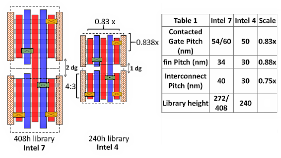
As shown in the above figure, individual features including the contacted gate pitch, the fin pitch, and the interconnect pitch have all shrunk by 12 to 25%. Another, previously announced innovation for this process node appears in the pink cross-hatched rectangles shown in the figure above. Those pink rectangles represent “dummy gates,” which are required to electrically isolate adjacent FinFETs. As depicted in the above figure, the dummy gates separate FinFETs located to the left and right. Previous Intel FinFET nodes use two dummy gates per transistor, but adjacent Intel 4 FinFETs share one dummy gate, which saves yet more real estate.
In addition, Intel 4 FinFETs need only three fins per transistor instead of the four fins per transistor required in the Intel 7 process. (Fins appear as horizontal gray rectangles in the figure above.) All other things being equal, the use of fewer, thinner fins would degrade performance because the FinFET’s channel resistance would be approximately 33% higher. However, Sell explained that Intel 4 uses cobalt-clad copper or “enhanced copper” for the chip’s lower metal signal layers, which reduces trace and gate impedance. Together with the additional capacitance reduction that results from scaling, Intel 4 FinFETs can get by with three fins without performance degradation.
The net result of these innovations is to double the number of transistors per square millimeter for chips made with Intel 4 relative to Intel 7. That’s the classic definition of the original Moore’s Law from 1965: a doubling of transistor density from one process generation to the next. In other words, Moore’s Law may have been dormant during the transition from planar FETs to FinFETs, but it seems to have roared back with Intel 4 – with one caveat. It’s much more expensive to fabricate a chip using EUV. The cost per transistor has been rising steadily since the days of planar FETs and 28nm process nodes, and transistor cost is most definitely a part of Moore’s Law. That part of Moore’s Law may be broken, bent, or dead, but transistor doubling seems to have returned.
Sell explained that Intel Foundry Services (IFS) customers will have access to the Intel 4 process, but that IFS is really concentrating on the follow-on process node, Intel 3. He also said that Intel will use even more EUV lithography steps in the Intel 3 process and will create a denser high-performance cell library specifically for that process node.
It will be extremely interesting to see whether Intel 4 or Intel 3 becomes the next process node for Intel FPGAs. Nothing’s been said yet. My guess is that it won’t be Intel 4 because Intel needs every bit of capacity from that node to counter the AMD client and server CPU threat. At the same time, FPGAs make excellent process pipecleaners, so it’s not impossible that some FPGAs might be made on Intel 4, though I think it unlikely.
Next-generation Intel FPGAs could easily target Intel 3, since that’s the one for which IFS will build capacity to manufacture chips and chiplets for volume customers. Note the word “chiplets.” Intel Agilex FPGAs already rely on Intel’s EMIB packaging technology to mix and match tiles from different process nodes, so it’s entirely possible that an Intel 3 FPGA chiplet could appear down the road.
However, neither node might be used to make FPGAs, at least for Intel. The Intel 3 node is, itself, an interim process step. Intel 20A, the first node in the company’s “Angstrom Era,” will replace FinFETs with RibbonFETs, which other semiconductor makers call GAA (gate all around) transistors. By stacking multiple transistor channels (ribbons) vertically on top of each other, RibbonFETs will significantly boost transistor density well above densities achieved by FinFETs, and this would be a very good thing indeed for infinitely expandable FPGA architectures. RibbonFETs also deliver better performance than do FinFETs because the RibbonFET gate completely surrounds the transistor channel. FinFET gates surround the transistor channel on only three of four sides, which means that FinFET gates have less control over current flow.
In addition, Intel 20A will be the company’s first process node to move the on-chip power distribution network (PDN) from the top of the chip to the back of the chip. This innovation should greatly reduce the PDN’s impedances and will therefore improve performance while simplifying signal routing on the chip’s top metal layers. The situation is entirely analogous to adding power and ground planes to a circuit board, which we’ve been doing since at least the 1970s. It merely took half a century to get this technology into ICs. This, too, would be a very good technology for making FPGAs, which are very sensitive to power supply noise and droop.
Intel calls this backside PDN technology “PowerVia.” Because a PowerVia PDN requires the creation of nano TSVs (through-silicon vias) in the wafer to supply power to the transistors, PowerVia is a more expensive technology for fabricating an on-chip PDN, but there are really big performance and signal routability gains to be had from this technology. Both aspects are at least as critical to successful FPGA design as they are for CPU design.
Adding PowerVia’s manufacturing costs to the extra costs associated with EUV lithography ensure that the average cost per Intel 4 transistor will not be heading down any time in the foreseeable future. Instead, it is likely to continue heading up, but that appears to be the price to be paid for reviving Moore’s Law, and it’s one that an Intel led by CEO Pat Gelsinger is clearly willing to pay.
Note: If you’re interested in the origins of Moore’s Law, see “Moore’s Law and the Seven Devices.”


Parts of this reads like an Intel PR; understandably, since it is among the industry leaders. As noted, the key factor is cost per switch [transistor], and that is at the right/riding edge of the bathtub curve – the ending.
When you change the base reference, from single chip to multi chip to 3D etc, and do not consider costs, one can extend such ‘laws’ ad infinitum. One could go full-wafer and claim to breakout of the doubling constraint of Moores’s.
I would like to collate Murphy’s law with Moore’s at some point. Something like a chip will keep getting larger and costs will keep rising.
Moore pulled off a good eponymy – or Intel did. After all it is at best a corollary to Wrights Law [experience curve].