editor's blog
Subscribe Now

Costs for Sub-20nm Wafers put Another Nail in Moore’s Law’s Coffin


IC Insights has just published the September Update to The 2018 McClean Report, and one figure (reproduced below) puts yet another nail into the coffin for poor old Moore’s Law. Now please take care. There’s a vertical line between the 200mm wafers on the left going down to 0.13 micron lithography and 300mm wafers on the right, going down to 20nm. Per-wafer costs more than doubled going from 0.13 microns to 90nm, but the available real estate on a 300mm wafer is more than twice that on a 200mm wafer, so the cost per square nanoacre of silicon has stayed pretty constant.

(Note that the figure is labeled “revenue” but that’s from the foundry’s perspective. To the foundry customer, it’s a cost.)

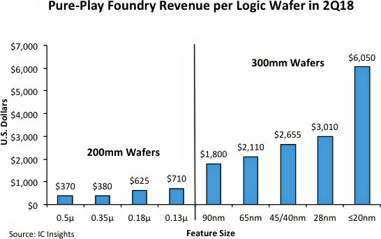
But look at the jump in per-wafer costs between 28nm and 20nm (and below). There’s a sharp cost jump of slightly more than 2x, with no increase in nanoacerage. Sure, you can get more chips per wafer thanks to shrinking feature sizes, but that’s not usually what happens. The next-generation chip always has to incorporate more features. That tall bar on the far right of the graph should be drawn as a nail because it’s going into the coffin lid for Moore’s Law, which is an economic law.

As a reminder, here are the words that Moore originally used to describe the phenomenon he was seeing back in 1965:


“The complexity for minimum component costs has increased at a rate of roughly a factor of two per year.”


Moore’s Law is not just about doubling. It’s about doubling component count at a minimum cost per component.

The latest McClean Report also says, “There will probably be only three foundries able to offer high-volume leading-edge production over the next five years.” Which three? TSMC, Samsung, and Intel. The cost of joining this club is so high, it’s a safe bet that no other company is going to apply. In fact, Globalfoundries just cancelled its club membership because the dues were becoming too high. (See “Monty Python, Dead Parrots, Moore’s Law, and the ITRS.”)


For more information about The 2018 McClean Report from IC Insights, click here.


One thought on “Costs for Sub-20nm Wafers put Another Nail in Moore’s Law’s Coffin”

Leave a Reply

featured blogs
Sep 19, 2023
What's new with the latest Bluetooth mesh specification? Explore mesh 1.1 features that improve security and network efficiency, reduce power, and more....
Sep 20, 2023
Qualcomm FastConnect Software Suite for XR empowers OEMs with system-level optimizations for truly wireless XR....
Sep 20, 2023
The newest version of Fine Marine offers critical enhancements that improve solver performances and sharpen the C-Wizard's capabilities even further. Check out the highlights: γ-ReθTransition Model and Extension for Crossflow Modeling We have boosted our modeling capabi...
Sep 20, 2023
ESD protection analysis is a critical step in the IC design process; see how our full-chip PrimeESD tool accelerates ESD simulation and violation reporting.The post New Unified Electrostatic Reliability Analysis Solution Has Your Chip Covered appeared first on Chip Design...
Sep 10, 2023
A young girl's autobiography describing growing up alongside the creation of the state of Israel...

featured video

TDK PowerHap Piezo Actuators for Ideal Haptic Feedback

Sponsored by TDK

The PowerHap product line features high acceleration and large forces in a very compact design, coupled with a short response time. TDK’s piezo actuators also offers good sensing functionality by using the inverse piezo effect. Typical applications for the include automotive displays, smartphones and tablet.

Click here for more information about PowerHap Piezo Actuators

featured paper

Intel's Chiplet Leadership Delivers Industry-Leading Capabilities at an Accelerated Pace

Sponsored by Intel

We're proud of our long history of rapid innovation in #FPGA development. With the help of Intel's Embedded Multi-Die Interconnect Bridge (EMIB), we’ve been able to advance our FPGAs at breakneck speed. In this blog, Intel’s Deepali Trehan charts the incredible history of our chiplet technology advancement from 2011 to today, and the many advantages of Intel's programmable logic devices, including the flexibility to combine a variety of IP from different process nodes and foundries, quicker time-to-market for new technologies and the ability to build higher-capacity semiconductors

To learn more about chiplet architecture in Intel FPGA devices visit: https://intel.ly/47JKL5h

featured chalk talk

The Future of Intelligent Devices is Here
Sponsored by Alif Semiconductor
In this episode of Chalk Talk, Amelia Dalton and Henrik Flodell from Alif Semiconductor explore the what, where, and how of Alif’s Ensemble 32-bit microcontrollers and fusion processors. They examine the autonomous intelligent power management, high on-chip integration and isolated security subsystem aspects of these 32-bit microcontrollers and fusion processors, the role that scalability plays in this processor family, and how you can utilize them for your next embedded design.
Aug 9, 2023
5,521 views