


There’s a new world order coming for the semiconductor industry, said A.B. Kahng. We’re racing to the end of Moore’s Law, and the race will now be won by sheer capex (capital expenditures) and size. Kahng, Professor of CSE and ECE at UC San Diego, was speaking at the Electronic Design Process Symposium (EDPS) held in September at the Milpitas offices of SEMI, the industry association for the global electronics supply chain.
The semiconductor industry’s tectonic plates are moving rapidly at the moment. Scaling levers—the ones that brought us to this point over the five decades since the initial formulation of Moore’s Law in 1965—they’re vanishing.
And just for the record, here are the words that Moore originally wrote:
“The complexity for minimum component costs has increased at a rate of roughly a factor of two per year.”
You see, Moore’s Law (now dead, see “Costs for Sub-20nm Wafers put Another Nail in Moore’s Law’s Coffin”) was never about speed or power. That was Dennard Scaling (observed in 1974, also now deceased). Moore’s Law is an economic law that predicts the cost per transistor in a monolithic integrated circuit. It predicts that per-transistor costs will see a decline of 1% per week, on average.
But not so much any more. This is the “Less than Moore” era.
Three macro-level factors drive the ultimate cost of a transistor in an integrated circuit: design, EDA tools, and manufacturing.
Macro Trend 1: Racing to the End of the Roadmap
Kahng then directed his attention to the macro trends driving the semiconductor industry today. The first macro trend is the race to the end of the semiconductor roadmap and the resulting new world order. We’re seeing more semiconductor vendors dropping back from the leading edge of semiconductor manufacturing. Case in point: Globalfoundries’ recent announcement that it was curtailing 7nm development (see “Monty Python, Dead Parrots, Moore’s Law, and the ITRS”). This development is just one of the latest road markers for this first macro trend.
Over the last couple of decades, the trend for IDMs (integrated device manufacturers) has been to move from vertical integration with captive semiconductor fabs—AMD’s former CEO Jerry Sanders III once said “Only real men have fabs”—to fab lite, to fabless. The heavy lifting in semiconductor process development is now in the hands of a very small number of heavyweight players, and most of the players are now foundries.
What’s driving this? Things are getting “ridiculously hard,” said Kahng. Signoff careabouts just keep mounting. “It’s getting worse no matter where you look.” Timing-driven place and route has become extremely difficult with the advent of FinFETs, due to the interactions between adjacent, on-chip devices. There are all sorts of new rules for device spacing in FinFET land, and none of these interactions have been modeled at 7nm.
Yet, the industry’s investment in EDA has been stable and small at less than 3% of semiconductor revenues. As a result, said Kahng, the cost for designing each square millimeter of chip real estate is now “out of control” and “EDA may be failing the industry.”
At the same time, the global market share for semiconductor consumption has been shifting to China, as Kahng demonstrated with the stacked-bar graph shown in Figure 1.
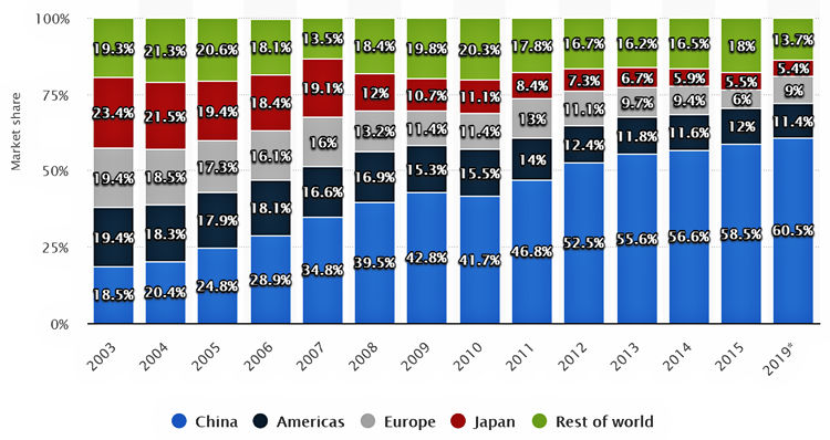
Figure 1: China’s semiconductor consumption as a percentage of the global market has risen in the past 15 years and is predicted to be 60.5% in 2019. (Image Source: https://www.statista.com/statistics/238228/global-semiconductor-market-share-by-region/)
As a result, fabs in China are sprouting like mushrooms to meet the growing domestic demand. For example, a recent YouTube video made by EEVblog’s Dave Jones discussed the availability of super-low-cost, Chinese-made microcontrollers from Chinese electronic component distributers. Think about buying OTP (one-time programmable) microcontrollers in relatively low volumes for three or four cents each, but don’t bother to think about buying such ultra-cheap parts locally, unless you’re in China. That’s just one tiny indicator of the rising New World Order for semiconductors.
Macro Trend 2: It’s the Methodology, Stupid!
The second macro trend, according to Kahng, is the rediscovery of design technology as an essential lever. Kahng reminded EDPS attendees of the workshop’s old tagline: “It’s the Methodology, Stupid!” To underscore this assertion, Kahng projected a graph from the 1993 ITRS Roadmap for Semiconductors, shown in Figure 2. This graph already contained an alert about the productivity gap, shown by the growing divergence between the red and blue lines.
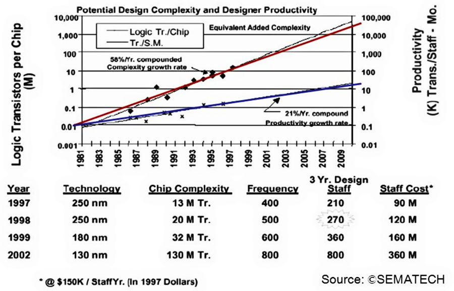
Figure 2: SEMATECH’s Roadmap from 1993 shows that design productivity was a major problem 25 years ago. (Image Source: Andrew Kahng)
In 2001, the ITRS Semiconductor Roadmap document stated that the “cost of design is the greatest threat to the continuation of the roadmap.” Even back then, design verification times had grown to months or years, with high uncertainty. Project deadlines were becoming fuzzier and fuzzier.
The 2013 edition of the semiconductor roadmap showed yet another gap—the available density gap. You can still scale transistors, but you can’t use them all when they’re packed together as closely as lithography allows because of the above-mentioned interactions between adjacent devices.
Put this all together and you get the dismal picture plotted by DARPA and shown in Figure 3. To my eye, the dots show a flattening of the historic increase in the number of transistors per chip along with a breathtaking rise in design and verification costs.
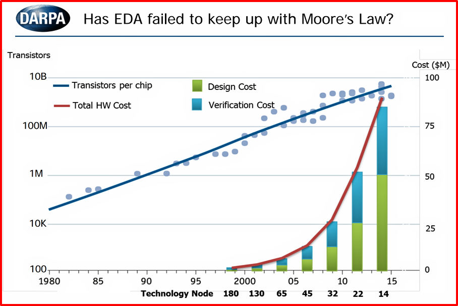
Figure 3: This DARPA graph from 2018 shows the exponential rise of design and verification costs versus semiconductor scaling. (Image Source: http://www.ispd.cc/slides/2018/k2.pdf, slide 8)
Kahng’s conclusion to this macro trend: “Wafer cost pretty much always ends up at a nickel or a dime per square millimeter in any process, but this curve… means that the cost of designing that square millimeter is out of control.”
Macro Trend 3: Extreme Consolidation
The third macro trend is extreme consolidation in the semiconductor industry. There are now only two main foundries, only two leading EDA companies, and only one leading lithographic supplier to the industry (ASML), said Kahng. There’s no such thing as an alternate source at technology’s bleeding edge any more.
As a result, there’s no longer much competition—not like there once was—and so the rules of the game have changed. There are fewer distinct customers for these suppliers; foundry-specific golden rules are hard-coded into the EDA tools; “and from my academic viewpoint,” said Kahng, “all this means that the foundry is increasingly well-positioned to become the Borg.”
Macro Trend 4: Chaos
Which brings us to the fourth macro trend: “More than Moore.” This macro trend takes the industry beyond lithographic scaling limits for monolithic devices and encompasses 2.5D/3D assembly, chiplets, and interposers. This path “includes too many options,” said Kahng. It is chaos. Worse, it’s chaos without adequate co-design tools for the chips and the 2.5D/3D assemblies.
Kahng then asked “What do we need the most?” His answer: new tools and automation; new standards including wrappers that allow interoperability among RF/analog die, digital logic, and memory die; new optimizers for IO planning and for marshalling high-speed interface signals across passive interposers. Finally, Kahng said, we need tools for design-space exploration, to avoid leaving value on the table.
Who’s Driving, Who’s Being Driven?
For the last 20 years, said Kahng, the foundries and designers held a lot of the cards. They had levers that could change yield Paretos in an instant. Designers could add custom cells, change signoffs, or modify manufacturing tests. The foundries reserved some wiggle room for themselves, while EDA basically added value only if the foundry and design had clearly failed. Foundry plus design WAS the semiconductor industry. EDA was just a supplier.
That said, some very nice, symbiotic collaboration has developed between foundries and EDA vendors over the past ten years. This has been the era of DTCO (design-technology co-optimization), but this collaborative era has been counterbalanced by one-to-one, encrypted, mutually exclusive relationships between foundries and EDA suppliers, resulting in hard-coded design rules for EDA at advanced nodes.
The collaboration has given us visibility into the ability to align these three facets:
- Design and foundry are alignable, which can result in special nodes, yield learning, and design services. Deep customer-supplier relationships can become partner relationships.
- Foundry and EDA are alignable, as evidenced by the strategic DTCO-type relationships that have developed.
- EDA and design are NOT fully alignable. We see this in the recent race to enable machine learning “in and around EDA.” Since its inception, EDA has always taken advanced design technology and methodology from leading customers and then wrapped it up, sold it back to the design community, and supported it. As design technology becomes more critical, people in the design community become less willing to reveal their secrets to other designers or to the EDA companies, and EDA development begins to stall.
“So, going forward, who will drive the scaling of cost and value?” asked Kahng. His answer: Foundry is the obvious suspect. Design is a longer shot because it’s now fairly removed from the silicon, separated by application and architecture. EDA can still add value, but it cannot drive cost scaling or value because it’s a supplier tied to the needs of foundries and design teams, in Kahng’s opinion.
I guess someone’s going to have to break all of this bad news to the EDA suppliers. They still think EDA is where electronics begin.
But don’t look at me. I’m not volunteering.


Steve, the biggest misnomer ever is the “design” in EDA. Design does not start with synthesis, place and route, and timing analysis.
First is functional specification/design. Then comes inputs, outputs, and what goes on inside to create outputs resulting from the inputs. Then the interface sequences/handshaking that define the input and output internal and external transfers. And this is all done by logic gates that can only be defined accurately by Boolean algebra.
All of this is totally ignored by the EDA tool chain that is totally obsessed with synthesis and possibly timing driven placement.
Also simulation is focused on creating waveforms from Verilog and VHDL. Now everybody uses the acronym RTL which is ambiguous to say the least. Yes there are registers and data moves along the data path where it may or not be manipulated, so what?
Microsoft had a successful project “Catapult” that was done in spite of the “tedious and frustrating” tool chain. They do not know it yet, but they are sitting on a solution based on the CSharp compiler API.
Possibly the most stupid conclusion ever was that since Verilog could be simulated, then it must be used for design entry.
I really wonder what design tools are really used where real products are actually created.
Allow me to clear up your question, Karl. Based on my years of experience, I know that the commonly used design tools all come from Acme, the very same company that supplies the Coyote in the Roadrunner cartoons.
All kidding aside, I agree with you. There’s clearly an uptake in the use of C/C++ to define hardware, but it’s really early days yet. C/C++ was developed as a procedural programming language and lacks the semantics to define parallelism without a lot of gymnastics. Just as the Inuit have fifty words for “snow” depending on the qualities of the white stuff and English has one word, “snow,” C/C++ lacks the subtle semantics (in my opinion) required to get the maximum potential performance out of programmable or ASIC hardware. I’ve yet to see anything that would make me believe otherwise although I expect something will come up in the future. Even today, for some specific applications, C/C++ works just fine as a hardware description language.
–Steve