


One transistor, two transistors, three transistors, four,
Five transistors, six transistors, seven transistors, Moore.
Way, way back in 1965, when the nearly prehistoric semiconductor industry made integrated circuits using the equivalent of stone knives and bearskins, Fairchild Semiconductor’s R&D Labs Director Gordon Moore wrote and published a very short article. If you have never heard of this article, check your browser. You have either fallen through a wormhole or you have been accidentally redirected from one of your friends’ Facebook or Instagram page, or some other, popular part of the Internet. However, assuming you belong here, you will have heard about and possibly will have read Gordon Moore’s article, titled “Cramming more components onto integrated circuits.”
Not a particularly monumental article title, is it?
However, the article’s impact was truly monumental. It was prophetic. It was the first public disclosure of a prediction that would eventually become known as Moore’s Law. Moore published his 4-page article in the April 19, 1965 issue of Electronics magazine, which was the electronics industry’s leading publication at the time. Moore’s brief article dictated the course of the semiconductor industry for the next 50 years – far longer than Electronics magazine managed to survive. (Electronics magazine published its last issue in 1995.)
Much has been written about Moore’s Law, which is based on the following graph from Gordon Moore’s article in Electronics:
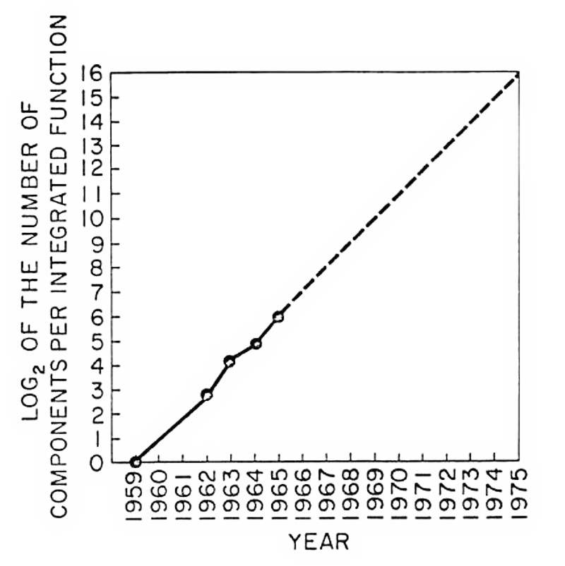
Using just five data points, based on component counts from actual devices, Gordon Moore was able to predict:
“The complexity for minimum component costs has increased at a rate of roughly a factor of two per year… Certainly over the short term this rate can be expected to continue, if not to increase. Over the longer term, the rate of increase is a bit more uncertain, although there is no reason to believe it will not remain nearly constant for at least 10 years. That means by 1975, the number of components per integrated circuit for minimum cost will be 65,000.
“I believe that such a large circuit can be built on a single wafer.”
(Note: Moore used a log2 scale for the vertical, component-count axis. Remember that fact; it will be important later.)
Gordon Moore was right. Oh brother, was he right. (Well, in truth, he was mostly right. A decade later, Moore revised his prediction from a 1-year doubling period to a 2-year doubling period, but the basic idea remained sound until recently, when we eventually needed to start cutting atoms in half to reduce device geometries by 50%.)
Although Moore’s Law – as it applies to planar, monolithic device scaling – has definitely run the last mile of its marathon, it had a profound economic effect on the semiconductor industry in particular, the electronics industry in general, and the world’s overall economy as well. That was no small feat for a 4-page article that appeared in a relatively obscure trade journal (as far as the public was concerned at the time) covering a relatively small (for the time) industry.
Over the past 50 years, many books and many, many magazine articles have discussed, analyzed, and reviewed Moore’s Law. I’ve written at least a dozen such articles myself. (Many of these articles erroneously credit Moore’s Law with semiconductor advances that rightfully belong to Dennard scaling: faster transistor speed and lower power consumption with each new process node.) At this point, you’d think there’d be nothing left to discuss regarding that original article on Moore’s Law.
But there is.
It’s been standing proud in the above graph for nearly 54 years. Do you see it? I didn’t. Not for years. Not until an article written by David Laws highlighted my own blindness.
For the past dozen years, Laws has been the Semiconductor Curator at the Computer History Museum in Mountain View, California. He’s also served as president or vice president at three semiconductor companies (Quicklogic, Altera, and AMD), so he’s got semiconductors in his blood. (Figuratively, not literally.) During the 1960s, Laws worked for SGS-Fairchild in the UK and then moved to Silicon Valley in 1968. So, Fairchild Semiconductor’s history is of particular interest to him, and he’s written many articles about that history.
Laws’s latest article, published on the Computer History Museum’s Web site, is titled “Madeleine Moment Connects Moore’s Law Artifacts.” This new article describes an artifact acquired by the museum in 2017. It is just a sheet of memo paper bearing Gordon Moore’s imprint with seven crudely drawn rectangles and some writing. There’s a small rip in the sheet of paper that’s been repaired with a yellowing piece of cello tape. This small artifact was donated by Sheila Sello after her husband Harry Sello passed away in 2017.
Harry Sello worked for Gordon Moore at the Fairchild Semiconductor Research Laboratory in Palo Alto, California during the 1960s. In his article, Laws writes:
“In 1967 Gordon asked Harry to prepare some 35 mm color slides illustrating this trend [Moore’s Law doubling] for an upcoming talk. Harry told me that he assembled a collection of chips that included Jean Hoerni’s 1959 single planar transistor plus the bipolar IC produced each year from 1962 to 1967 that met the minimum cost per component criterion.”
That’s the criterion Gordon Moore used to select the devices that he represented on the graph in his 1965 article. Moore’s Law is about semiconductor device density and cost. Two years later, Sello collected the requested semiconductor die and shot a group photo. That photo appears in Laws’s article and below, reproduced here with permission from the Computer History Museum.
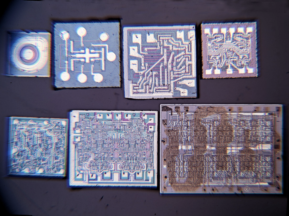
Harry Sello’s 1967 photograph of the five Fairchild semiconductor chips that Gordon Moore used to plot the graph that predicted Moore’s Law. (Image credit: Computer History Museum)
Ten years ago, while Sello worked as a Computer History Museum docent, Laws asked him about his photo. It had become part of the museum’s collection, and Laws was researching the history of Moore’s Law for the museum’s Silicon Engine online exhibit. At the time, Sello could recall the identities of a couple of the chips in his photo, but he could not remember all of their names nor their dates of manufacture.
Years later, when he saw the newly acquired memo written on Gordon Moore’s note paper, the penny dropped for Laws, who writes:
“Having worked at Fairchild in the 1960s, I immediately recognized several of the part numbers from the catalog of that era. As Harry had repaired a tear in the paper and held on to it for 50 years, it must have been important to him. While trying to decipher the notes in Gordon’s … and Harry’s … cryptic scrawl, something familiar about the arrangement of the rectangles triggered my Madeleine Moment. This was the Rosetta Stone to the device types in that 1967 photograph and the first five appeared to match the years of the devices on the plot … from the 1965 article.”
When I read this paragraph in Laws’s article, I realized that I’d never really wondered about the specific devices that Gordon Moore used as the basis for formulating Moore’s Law. It never mattered or even occurred to me that the 1965 graph did not list these devices by part number. The graph in Moore’s 1965 article lists only the component counts for the devices, and only in log form. (Nice bit of nerdery, that, but it’s how you plot a straight line using exponential data.)
In my opinion, Moore’s graph is likely the most important graph ever plotted in the history of semiconductors, and the devices used for its five data points are completely anonymous. After reading Laws’ article, I suddenly became extremely curious about the devices that provided the five data points Moore used to plot this graph. They’ve remained nameless for more than half a century.
No longer.
Laws’s article lists the devices plotted on Moore’s graph and pictured in Sello’s photo. However, Laws’s article supplies only a little information about the seven devices pictured in Sello’s photo and the five devices used in Moore’s graph. As it turned out, each of the seven devices is significant in its own right (and, of course, all were made by Fairchild), so here’s a more in-depth description for each of the seven devices:
Device #1: Fairchild 2N697 NPN, 150mA, 60V, bipolar transistor, 1 component, circa 1959.
The plotted curve on Moore’s graph from his 1965 article begins with a 1-component semiconductor device in 1959. That’s a transistor. In 1957, the Traitorous Eight exited Shockley Semiconductor Laboratory located at 391 San Antonio Road in Mountain View, walked about a mile up the street, hung a left on Charleston, and founded Fairchild Semiconductor. They’d left a shocked William Shockley specifically to focus on making silicon transistors because Shockley had refused to let them do it. (See “For Lease: Birthplace of the IC” and “391 San Antonio Road: The House that William Shockley Built (and Destroyed).”)
Fairchild Semiconductor’s first commercial semiconductor products were the 2N696 and 2N697 silicon transistors. The two transistors were identical parts, sorted and binned by testing for current gain. (The 2N697 has double the current gain compared to the 2N696, so the best transistors were stamped “2N697” and the rest got the “2N696” stamp.) The two transistors were the first commercially available semiconductor devices to be made with the mesa process, using photolithography and double-diffused junctions developed by physicists, chemists, and engineers instead of grown alloy junctions made with heat, small drops of liquid antimony or indium, and a big dollop of alchemy.
Fairchild shipped prototypes of the 2N697 transistor to IBM’s FSD (Federal Systems Division) in 1958. They were destined to be used as magnetic-core memory drivers in the on-board computer that IBM FSD was designing for North American Aviation’s ill-fated XB-70 Valkyrie bomber. However, the transistors themselves were not ill-fated. Far from it. Fairchild commercialized the 2N696 and 2N697, and the first ad for these transistors ran in August, 1958. The prototypes reportedly cost IBM $150 a pop. A legion of semiconductor manufacturers quickly copied these devices. You can still buy 2N696 and 2N697 transistors, by the way. However, they no longer cost $150 each; they’re not made with the mesa process any longer; and you won’t be buying them from Fairchild.
The 2N697 is the only pre-IC semiconductor device on Moore’s graph. Fairchild Semiconductor built the first integrated circuit in 1959 by extending the photolithographic concepts used to fabricate the 2N696 and 2N697 transistors. The improved process became known as the planar process. Fairchild’s planar process is still the bedrock foundation of the entire semiconductor industry.
![]()
The Fairchild 2N697 NPN, bipolar, transistor was the first commercially successful silicon transistor. It was made with the diffusion-based mesa process rather than the older alloy process. Note the Fairchild “Flying F” logo stamped into the top of the package. (Image credit: The Transistor Museum)
Device #2: Fairchild μLogic Type G RTL IC, 7 components, circa 1962.
An article from the October 1, 1960 issue of EDN magazine reads:
“High-speed, low power digital computer logic building blocks are under development at Fairchild Semiconductor Corp. To be available early next year, the family of solid-state micrologic elements will handle all the logic function requirements of a digital machine, no other components being required.”
The article lists six IC element types being developed for the µLogic family including:
- “F” Element – Flip-Flop
- “S” Element – Half-Shift Register
- “G” Element – 3-Input NOR Gate
- “B” Element – Buffer
- “H” Element – Half Adder
- “C” Element – Counter Adapter
These six IC elements form the first IC logic family, Fairchild’s initial RTL (resistor-transistor logic) series. (Note that “RTL” does not mean “register-transfer level” in this context. That’s a more recent overloading of the term.) These RTL parts were later renamed Fairchild’s μLogic 900 and then 9900 series.
ICs were not a sure thing in the early 1960s. The EDN article from 1960 notes:
“The weight and size of batteries and solar cells is the main problem in missile and space electronics – not the size of the electronics package…
“Whether standard modules are practical or not is still a point of controversy within the industry.”
However, weight and size of the electronics package were both very critical parameters for one specific space program, code named “Apollo.” NASA tasked MIT’s Instrumentation Lab with developing the AGC (Apollo Guidance Computer) to navigate and land astronauts on the moon and to return them safely. The Instrumentation Lab realized that the AGC’s size and weight would be extremely limited, which meant that the computer’s designers needed to develop the AGC using revolutionary, lightweight, miniaturized electronics technology.
On February 27, 1962, MIT’s Instrumentation Lab ordered 100 Fairchild μLogic Type G ICs at the price of $43.50 each (in 1962 dollars!) for evaluation. Within a few months, the MIT Instrumentation Lab concluded that, yes, ICs were a very good thing to use for the Apollo Guidance Computer and used 4100 of them to implement all of the logic in the AGC’s Block I design. By 1965, the AGC program had purchased some 200,000 Type G logic chips at an average price of $20 to $30 each. Game on!
Device #3: Fairchild μLogic Type R, D-type RTL Flip-Flop, 33 components, circa 1963 or late 1962.
The third device in Sello’s 1967 photograph is a Fairchild μLogic Type R, a D-type flip-flop that presents an additional mystery relating to the graph in Gordon Moore’s 1965 article. Based on the third die in Sello’s photograph, the Fairchild μLogic Type R flip-flop has too many on-chip components to be the third device plotted on Moore’s graph. Laws writes:
“How to explain the 1963 Type R that appears as an outlier with the Log2 value of 5.0? With 33 components, it is as complex as the 1964 device [on Moore’s graph]. The value of 4.2 for the year 1963 on the original plot equates to 18 components on the chip. The best candidate for that is the [μLogic] Type S (Half-Shift Register) with 10 transistors and 8 resistors. One explanation is that Harry was unable to locate a Type S [die] for the photo and substituted a Type R that was more complex but fabricated with the same technology.”
The Type S Half-Shift Register was one of the original six elements of Fairchild’s μLogic RTL family. The Type R flip-flop was not. I’ve struggled to find a good definition of a Half-Shift Register. I’d never heard of such a thing in my logic-design days and here’s the best definition I could find using Google:
“It takes two of these to make one stage in a shift register.”
I guess that’s all you or I really need to know?
Actually, with a little help from David Laws and some additional research, it’s clear that the Type S Half-Shift Register contains the logic needed to serve as either the master or slave latch in a master-slave RS flip flop. A master-slave flip-flop also needs an inverter or an inverting gate to invert the clock to the slave latch, so it appears that you’d need three RTL ICs to build a master-slave RS flip-flop: two Type S Half-Shift Registers and one inverting buffer (or a discrete transistor). This explanation conveniently leads to the next device in Sello’s photo.
Device #4: Fairchild DTL 945 Master-Slave Clocked RS Flip-Flop, 34 components, circa 1964.
The first two ICs on Moore’s graph (devices #2 and #3) were RTL chips. The fourth device is a DTL (diode-transistor logic) clocked RS flip-flop with all of the logic needed to implement a master-slave device. The Fairchild 945 (later, the 9945) clocked flip-flop was part of the company’s 930 DTL logic family (later renamed the 9930 series).
The first-generation RTL ICs were quite successful, but they quickly became outdated because they were too slow and drew too much power. (Nothing’s changed in 50 years, has it?) Clearly, RTL ICs would be supplanted quickly and DTL was the first logic family to try for the brass ring.
Signetics, founded in 1961 by a renegade group of Fairchild engineers who wanted to focus exclusively on ICs when Fairchild’s management wouldn’t let them do it (sounding familiar?), developed the SE100 DTL logic family as its first standard product line. Announced in 1962, the SE100 DTL logic family bit into Fairchild’s RTL market. The machine that was Fairchild countered with the 930 DTL logic family, which offered better performance specs and lower prices than Signetics’ DTL parts thanks to Fairchild’s superior lithographic and process technologies. The result was predictable.
Fairchild’s 930 DTL logic family bit back and dominated the logic market for years, until the TTL wars erupted. The 930 DTL logic family became a huge commercial success. Fairchild succeeded in dominating both the first and second IC logic generations with its RTL and DTL logic families.
Device #5: Fairchild CμL 958 Decade Counter, 58 components, circa 1965 or late 1964.
Now we’re getting into some serious integration. Fairchild’s 958 (subsequently renamed the 9958) Decade Counter appeared during the heyday of Nixie displays. Everyone in the instrumentation business during the 1960s coveted the warm, orange, digital glow of Nixie-tube readouts for their counters, timers, and digital voltmeters. If you wanted your equipment to look modern in the 1960s, you just needed to sprinkle a little Nixie dust.
All of these instruments needed digital decade counters to drive the Nixie displays, so it was plainly obvious to Fairchild’s engineers that they needed to put an entire 4-bit decade counter in an IC package as soon as possible. The result was the Fairchild CμL 958 Decade Counter. (The “CμL” designation stands for “Counting Micrologic,” of course.)
Finally, we have the two ICs that do not appear in Gordon Moore’s 1965 chart but do appear in Sello’s 1967 photograph. They are:
Device #6: Fairchild 9300 4-Bit Universal Shift Register, 125 components, circa 1966.
Fairchild’s 930-logic family managed to become king of the DTL hill, but soon a scene-stealing competitor called TTL (transistor-transistor logic) appeared on the stage. TTL logic functions were faster than equivalent RTL and DTL functions due to several inherent circuit advantages, and speed was the name of the game. (It still is.)
There was a ferocious race to develop new logic families capable of becoming the industry’s top TTL dog. Fairchild developed the 9300 series (10x better than the 930 DTL family, perhaps?), which included the 9300 4-bit universal shift register IC. Why is it universal? It has an asynchronous reset input pin. It has a parallel load feature using four parallel input pins. The register’s four output bits are likewise available on output pins. It shifts left or right, if you wire it correctly, to exploit the parallel-load feature. It slices; it dices; and it juliennes.
Alas, by 1967, Texas Instruments’ year-old, low-cost, plastic-packaged 7400 TTL family was burying Fairchild’s 9300 TTL family and, adding insult to injury, TI produced pin-for-pin replicants of Fairchild’s best 9300-series designs and slapped 7400-series part numbers on them. Want proof? If you know your 7400-series TTL Data Book, you may recognize the 9300 4-bit Universal Shift Register as TI’s 74195 4-Bit Parallel-Access Shift Register. Similarly, Fairchild’s 9341 ALU became far more widely known as TI’s 74181 ALU.
Device #7: Fairchild Micromatrix 4500 DTL, Mask-Programmable, 32-Gate, Gate Array, 264 components, circa 1967.
Truly, I’ve saved the best device for last. The Fairchild Micromatrix 4500 was the industry’s first commercially successful, mask-programmable gate array – introduced all the way back in 1967! (The Star Trek episode “City on the Edge of Forever” that I obliquely referenced in the first paragraph of this article originally aired in 1967.) The Micromatrix 4500 Gate Array – it’s really the world’s first commercially successful ASIC – incorporated a whopping 32 uncommitted 4-input AND/NAND gates (the output inverter could be omitted using appropriate mask wiring) that you’d connect up using two metal mask layers.
Fairchild introduced early EDA software including the FAIRSIM logic simulator and automatic placement and routing programs to help designers lay out the metal interconnect for the Micromatrix 4500 Gate Array. Several Fairchild customers developed custom ASIC designs based on the device. In addition, Fairchild tried developing a few standard devices for its own product catalog using the 4500 Gate Array as a master slice.
David Laws sent me a photograph of the Micromatrix 4500 Gate Array die. It appears below.
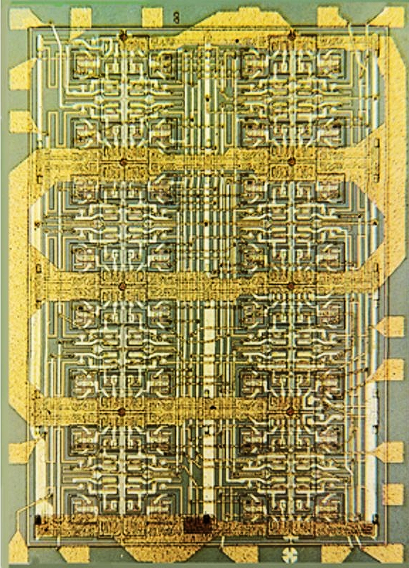
Fairchild Micromatrix 4500 DTL Gate Array (Image credit: Courtesy of David Laws)
Laws estimates that the Fairchild Micromatrix 4500 Gate Array incorporated 264 components, based on his visual assessment of the above die photo.
Today’s behemoth chips fabricated with nanometer lithography incorporate several tens of billions of transistors plus many more assorted electronic components. We’ve needed only fifty years to go from two hundred components on one semiconductor die to tens of billions. By any yardstick that you might care to use, that’s a stunning achievement, and Gordon Moore predicted all of it in 1965 with the merest whiff of data – just five data points – and a massive intuitive leap.


Moving the goal post from one year to two years to make the graph fit is typical forecasting. And he was just postulating a growth of complexity – to later come back and call it a ‘law’ seems like an interesting PR coup. When did the term Moore’s Law first appear? Who used it? My guess is some Intel pronouncement.
Intel did not even exist when Moore wrote his article. He was working for the company he founded previously, Fairchild. Also, he didn’t call it Moore’s Law. Caltech professor Carver Mead popularized the term “Moore’s law” in 1975, ten years after the article appeared. Mead was another luminary in the semiconductor field.
To add to what Steve said, the change from one year to two also didn’t happen until ten years after the article. And, in the article itself Moore said the trend could be expected to continue for at least ten years, so the change was actually more of a follow-on prediction after the first ten year forecast had proven true.
This week Meyhofer and Reddy published research that might well extend Moore’s Law another several decades. https://news.umich.edu/running-an-led-in-reverse-could-cool-future-computers/
On die cooling by reverse biasing an IR led so that it absorbs IR photons rather than emitting them.
There are several obvious ways to make this really effective toward extending Moore’s Law.
1) place these nano coolers right up against the hottest circuit features (IE high frequency) to manage the thermal gradient across the die
2) layer these nano coolers in 3D to cool active circuits both above and below the nano cooler, enabling 3D IC construction that was previously limited because we couldn’t get the heat out of the middle structures, and would generate high on die thermal gradients … and thermal noise. No longer talking about a single layer of FinFET’s … but possibly dozens where lower power layers of static RAM are sandwiched with nano coolers and high frequency logic.
3) use heavy … very heavy metal layers for both heat spreaders and stable voltage planes in the nano cooller and active logic layers.
>Device #2: Fairchild µLogic Type G RTL IC, 7 components, circa 1962.
This is a 3-input NOR gate, available in a TO-99 8-pin can, although you could buy a version where two of the pins were cut off (package code 5C). The die shown is the original non-epitaxial process where the base resistor of about 125 ohm is part of the NPN transistor. The collector resistor is about 600 ohm. Interestingly, the die shown has four transistors along with a corresponding fourth input, meaning that a 4-input NOR gate could be implemented, although this part was not listed among the initial RTL family. This die only has five components with four transistors and one collector resistor. As the base resistor is part of the transistor, you can’t really count it as a separate part. You can also see this die in [1], where the fourth input is not connected.
The most complex part of the original non-epitaxial family (also available in 1962) is the half-shift or S circuit (later called 905 or 9905). This is a gated RS flip-flop which uses four 2-input NOR gates. The clock input is also inverted so that it could be used with another half-shift to implement a master slave flip-flop (so no need for another inverter). This circuit used nine transistors and five resistors, for a total of 14 components with log_2(14) = 3.8. Was Moore cherry picking his data?!
In 1963, Fairchild redesigned their RTL family to use their much better epitaxial process [2,3]. Here the base resistor was now a separate component at about 450 ohm with a collector resistor of about 640 ohm. The G 3-input NOR gate was later renamed to the 903, then 9903 and then back to 903 in the 1970s. A 4-input NOR gate called G1 was also available, later called the 907 or 9907. A half-shift without the clock inverter was also available as the 906 or 9906.
The most complex part of the initial epitaxial family was also the 905 half-shift with nine transistors and 14 resistors, giving a component count of 23 or log_2(23) = 4.5. In 1964, Fairchild released a JK flip-flop called the 916 [4]. This has 12 transistors and 16 resistors for a component count of 28 or log_2(28) = 4.8.
>Device #3: Fairchild µLogic Type R, D-type RTL Flip-Flop, 33 components, circa 1963 or late 1962.
This device used low power epitaxial RTL, as indicated by the long length of the resistors. Typical resistor values were 1.5 kohm for the base and 3.6 kohm for the collector. The earliest information I have on this device is from May 1964 [6], where it is listed as the 913 but does mention the R or Register designation being used previously. This used 15 transistors and 20 resistors for a component count of 35 or log_2(35) = 5.1.
>Device #4: Fairchild DTL 945 Master-Slave Clocked RS Flip-Flop, 34 components, circa 1964.
The earliest information I have on the 945 is from April 1965 [7]. This is actually a master-slave flip-flop. The 931 master-slave flip-flop from December 1964 [8] preceded the 945. The 931 was difficult to use as the set and clear inputs were not fully asynchronous, which was corrected in the 945. The 931 used 14 diodes, 12 transistors and 22 resistors for a component count of 48 or log_2(48) = 5.6. The 945 has 16 diodes, 13 transistors and 21 resistors [9] for a component count of 50 or log_2(50) = 5.64.
>Device #5: Fairchild CµL 958 Decade Counter, 58 components, circa 1965 or late 1964.
The earliest date I have for the 958 is June 1966 [10], which used RTL. Unfortunately, the complete schematic is not shown, but it has at least 56 components, with 14 components for each register. The components for the clock buffer and 2-input AND are not shown.
In summary. Some of the dates may be earlier.
Date Count Device
1962 14 S Non-Epitaxial Half-Shift
1963-10 23 S (905) Epitaxial Half-Shift
1964-05 35 R (913) D-Type FF
1964-05 28 916 JK FF
1964-12 48 931 Master Slave FF
1965-04 50 945 Master Slave FF
1966-06 >56 958 Decade Counter
[1] The Inside Story on Fairchild Micrologic, 1962.
https://www.computerhistory.org/collections/catalog/102762881/
[2] Fairchild Epitaxial Micrologic, 1963.
https://archive.org/details/bitsavers_fairchildmpitaxialMicrologic1963_1941938
[3] W. O. Hamlin, “10-Mc Epitaxial Integrated Functional Blocks,” Fan-Out, No. 114, Oct. 1963.
https://archive.org/details/fairchild-fan-out-no.-114-oct.-1963
[4] W. O. Hamlin, “J-K Flip-Flop Integrated Circuit,” Fan-Out, No. 116, Feb. 1964.
[5] G. W. A. Dummer, “American Microelectronics Data Annual 1964-65,” 1964.
[6] Fairchild Semiconductor, “MWµL, Planar Epitaxial Milliwatt Micrologic Integrated Circuits,” May 1964.
https://archive.org/details/fairchild-mwu-l-may-1964
[7] G. Powers, “Diode-Transistor Micrologic Integrated Circuits,” Fairchild Semiconductor Application Bulletin APP-107, Apr. 1965.
https://archive.org/details/fairchild-app-107-apr.-1965
[8] Fairchild Semiconductor, “DTµL 931 Clocked Flip-Flop, Fairchild Diode-Transistor Micrologic,” Dec. 1964.
https://archive.org/details/fairchild-dtu-l-931-clocked-flip-flop-dec.-1964
[9] Fairchild Semiconductor, “Fairchild Diode-Transistor Micrologic Integrated Circuits, Industrial Microcircuits-Composite Data Sheet,” SL-253, June 1966.
[10] G. Powers, “Counter Micrologic IC – A New Dimension In Multi-Function Elements,” Fairchild Semiconductor Application Bulletin APP-118/2, Jun. 1966.
https://archive.org/details/fairchild-app-118.2-jun.-1966
Steven, thank you for this additional information!
Thanks! I’m glad you found the information useful. A small update.
I found a schematic for the 958 RTL decade counter [11]. This shows only 12 components per register (two clock input resistors were deleted), 7 components for the clock buffer and 3 components for the AND gate, giving a total of 58 components, agreeing with your value. However, the 958 is not the most complex device of the CµL family! The 959 RTL quad latch has 16 components per latch and 7 components for the enable buffer, for a total of 71 components.
The July 1969 issue of Electrical Design News showed the prototype F SR FF [12]. This had four transistors and two resistors for a component count of six. Note that the production F circuit used a different layout and pinout [13].
Date Count Device
1961-07 6 F Prototype Non-Epitaxial RS FF
1962 14 S Non-Epitaxial Half-Shift
1963-10 23 S (905) Epitaxial Half-Shift
1964-05 35 R (913) D-Type FF
1964-05 28 916 JK FF
1964-12 48 931 Master Slave FF
1965-04 50 945 Master Slave FF
1966-06 58 958 Decade Counter
1966-06 71 959 Quad Latch
[11] Fairchild Semiconductor Integrated Circuits, 1966.
http://madrona.ca/e/FSIC1966/FSIC1966-1632.pdf
[12] R. H. Norman and R. C. Anderson, “Micrologic Elements, Their Applications in Circuit Design,” Electrical Design News, pp. 44-46, Jul. 1961.
https://www.bitsavers.org/components/fairchild/micrologic/Fairchild_Micrologic_EDN_Jul1961.pdf
[13] Fairchild Semiconductor, “µLF Flip-Flop Element Tentative Specifications,” Nov. 1962.
https://archive.computerhistory.org/resources/access/text/2017/01/102770285-05-01-acc.pdf