


The upshot: Memories can be arranged such that an “access” becomes a multiply-accumulate function. Storing weights in the memory and using activations as inputs saves data movement and power. And there are multiple ways to do this using RRAM, flash, and SRAM – and then there’s an approach involving DRAM, but it’s completely different.
In the scramble to win the artificial-intelligence (AI) lottery, numerous companies are trying to create the best machine-learning (ML) engines. That means the fastest inference with the lowest power, and the lowest-power thing means figuring out how to avoid “hitting the memory wall.” In other words, a huge amount of power is spent moving all the necessary data around. And we’re talking into the billions of pieces of data.
We saw part of this a couple of weeks ago, with new inference architectures that have an emphasis on memory bandwidth and locality, trying to move less data faster and with lower power. But we intentionally put off discussion of a rather different way of solving this problem: in-memory computing.
In a more traditional architecture, you have some arrangement of multiply-accumulate (MAC) circuits for use in tensor math – specifically, matrix multiplication (with its own acronym: GEMM, for “general matrix multiplication”). These architectures try to arrange the MACs in a way that accommodates the need to move weights and activations into place. The activations are calculated by the prior neural-net layer (with the first layer using the actual network inputs as “activation”), while the weights are stored… somewhere. The multiplication generally involves activations and weights, so both must be moved to whichever engine(s) will be multiplying them. That’s the crux of the problem.
In-memory computing leverages a rather convenient fact of memories, such that, if you store weights in a memory, you can get a multiply-accumulate by accessing the memory with the activations. The only difference from a real memory is that you engage all word lines at once, rather than decoding the input to get only one word line going.
What we’re doing here is moving into the analog domain, treating the memory cells as analog elements rather than digital ones, in order to lower power. We already saw one approach to using analog in the front end of an inference engine; in-memory computing uses it in the memory. So we take digital data, turn it into analog values using DACs, drive the memories, which have analog contents, with those analog values to get an analog bit-line output, and then we use ADCs to convert that result back into a digital format.
We’re going to dig into the specifics of the different technologies, but, given all that there is to talk about, there will be lots of detail omitted, for which I refer you to the links at the end.
Doing it with RRAMs
We talked about this in general earlier this year, and then we looked more specifically at how this might be implemented in a resistive-RAM (RRAM or ReRAM) memory or using ferroelectric FETs (FeFETs). But, while RRAMs have been the most commonly described way of doing this – partly because it’s so easy to understand by applying Ohm’s Law to an array of resistors – there are issues with relying on an RRAM future for this.
As told by folks working on alternatives, RRAMs still require development work to bring them to commercialization. And the relationship between programming and resistance is non-linear, leading to even more work to make a commercially viable RRAM in-memory computing circuit. In other words, “Great idea, but call us when you’re ready.” I’m certainly not aware of any commercial development (as opposed to pre-commercial research); feel free to comment if you believe otherwise.
So, if we’re not ready to do this with an array of resistors, then what do we do?
Doing it with Flash
The next approach I’ve heard about uses flash memory instead of RRAM. NOR flash, to be specific, as it has a more traditional word-line/bit-line structure. At first I was intrigued by a comment that these use a capacitive rather than a resistive approach. Does the multiply-accumulate math work equally well there, using something other than Ohm’s Law?
Well, actually, it is resistive – and capacitive. Normally the bit cell is a transistor that’s on or off. But if it’s partially on, then it acts as a resistor – and the resistance is determined by the amount of charge on the floating-gate of the bit cell (a capacitor). When it’s all the way on, the cell conducts to its capacity. All the way off, and it doesn’t conduct at all. Partially programmed, and, well, it conducts some. Microchip provided the following graph to illustrate the linear nature of resistance in the in-between programmed states.
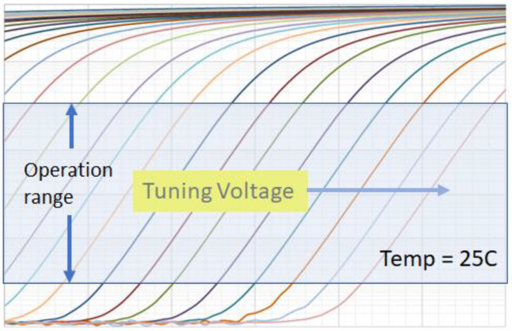
(Image courtesy Microchip Technology)
For those of you familiar with flash, this may sound similar to something you’ve seen before. This is like MLC or TLC bit cells on steroids. You may recall that these are two ways to store more info in a single flash bit. MLC, or “multi-level cell,” stores 2 bits. That means that programming can take on four different levels, including all-on and all-off. TLC means “triple-level cell,” and it stores 3 bits using eight levels.
Well, in principle, it’s not hard to extend this to “ILC” – if I may be so bold – for “infinite level cell.” In other words, rather than 4 or 8 discrete levels, it’s a continuous range. To be clear, no one is using – or proposing – the ILC name, but, hopefully, you get the idea. And, in practice, the number of levels in the cell may not be much more than what’s used in a TLC cell. So the whole continuum thing helps us to understand what’s going on, but the reality is rather more limited at present.
If we go down to basic physics, of course, we can’t do an infinitely continuous cell. That’s because the gate value is discrete: it’s determined by the number of electrons in the floating gate (or charge trap). You can’t have fractional electrons, so the range of cell resistance values is effectively quantized. But, in practice, there are lots of electrons – and the electrons aren’t counted during programming, so their number is a plus-or-minus thing.
If one were to leverage a small, leading-edge flash cell, then the number of electrons starts to matter. But, with older technologies, and, potentially, with larger-than-typical cells to host more electrons (since storage density isn’t the main goal here), you can still deal with a large pool of electrons, plus or minus.
This gets us into the topic of challenges with this approach. You can’t control the number of electrons precisely. And the response to whatever number there is will vary by process and temperature and all of the variables that contribute to variation. So that nice, clean graph above gets a bit messier in practice.
There are two companies going down this road. Microchip has their memBrain array (a pretty clever name, you must admit), courtesy of their SST acquisition, and Mythic is a startup working on an inference engine that employs in-memory computing with flash. (Mythic licensed their flash, but they declined to say from whom.) And both companies say that they’re battling the variation using a wide range of calibration techniques (the details to which I have not been made privy).
It’s one thing to calibrate at startup (or even at test), but flash cells also lose electrons over time. That’s why flash memory has a data-retention spec. Electrons will willy-nilly tunnel out here and there because they’re bored or something. Which brings up an interesting topic: what are the meanings of data retention and its cousin, endurance, on this type of memory array?
From an application standpoint, it partly depends on whether this is going to be used in a cloud or edge inference engine. At the edge, it’s likely to be doing some fixed inference function for the life of the device. So, if there are enough of these arrays, then you load the weights in the first time, and, given that flash is non-volatile, you never have to program them again (unless you have an in-field update). While you still have to move activations around, you’ve completely eliminated the need to move weights; they’re permanently stored in the arrays.
In the limit, that would suggest that endurance – the number of times a device can be programmed before accumulated damage hastens the leakage of electrons to an unacceptable level – would be irrelevant. It’s going to be programmed only once.
In a cloud application, by contrast, the device is likely to be shared as a general compute resource, so it will need to be reprogrammed for each new application that comes its way. That means that, in the cloud, endurance becomes much more important. Mythic claims 10K write cycles, with the observation that, even if you reprogrammed daily, it would still last over 10 years. Microchip also anticipates endurance of 1K – 10K cycles.
Then there’s data retention in general. A standard flash cell is a great illustration of the noise-immunity benefit that digital provides over analog. You can lose (or gain) some electrons in a simple one-bit cell, and it won’t matter. The cell will still read the same. And it will do so until too many electrons crawl away like unsupervised infants.
But if we’re using an analog value on the gate and an analog value in the cell, then, in theory, every electron matters. Yes, there’s some wiggle room, but, if enough electrons migrate, then either you need to refresh the cell, or… you need somehow to compensate for the changed behavior of the cell, since the same analog input will create a different result today than it did a year ago.
Some aging is also handled by calibration circuits. But, for data retention, Mythic says that they do perform “… periodic background refresh of the weight values stored in the flash.” This would make endurance the dominant wear-out mechanism rather than data retention. Microchip says its data retention is TBD, but likely sees the devices being reprogrammed quarterly or yearly to restore the cells.
These guys have also spent a lot of energy on the DACs and ADCs. They need lots of them (Mythic says they have 27,000 ADCs). They need to be of high quality to keep the signal-to-noise ratio (SNR) in a range that promotes accurate inferences, and this is where a lot of the design effort has gone. Mythic claims a novel ADC; Microchip can share their ADCs to reduce the number needed. While the ADCs do consume energy, both claim that their use reduces overall system power by a large margin.
Microchip’s full array structure is shown below.
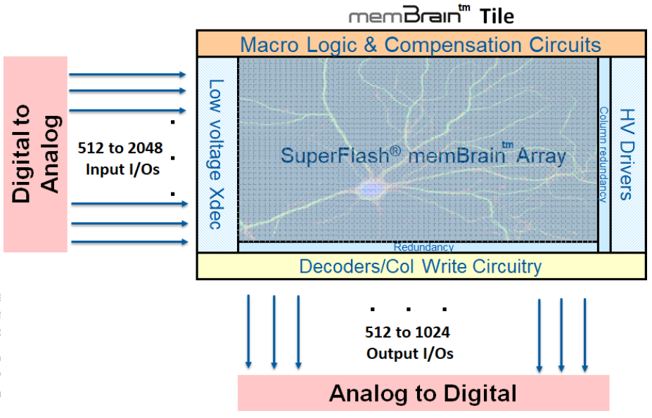
(Image courtesy Microchip Technology)
Microchip is selling their memBrain tile as IP for others to integrate into their inference chips. Mythic, on the other hand, is using theirs in their own SoC. They use slightly different terminology – compute-in-memory and analog computing – but it’s the same beast. Our focus with them today will stop with the memory array; we’ll look at their full architecture in a future piece.
I’m going to detour briefly into my own musing here, wondering if other cell technologies could be employed in this way. If you could get partial melting/crystallization of PCRAM cells, then might that would work? MRAM sounds like it wouldn’t work, given the strict north/south orientation of a magnetic domain, but it’s not that simple. The nature of the programming is determined by the amount and angle of aligned dipoles, which could be something other than 100% and something other than parallel or anti-parallel. So this could also, ideally, take on an analog value as well. I had a quick conversation with an MRAM industry expert who said that, theoretically, it might be possible, but it hasn’t been shown to be practical. To be clear, I’m unaware of any specific ongoing projects involving either of these technologies.
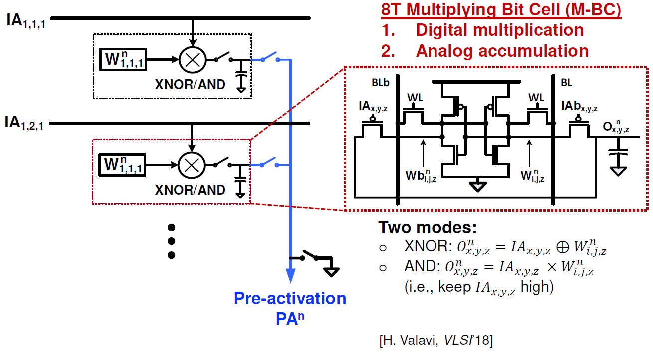
Doing it with SRAMs
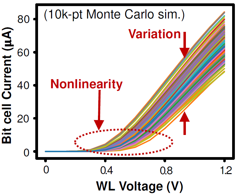
The next idea comes from a Princeton University presentation at Hot Chips. It uses SRAM arrays. Which might seem… surprising, since they’re volatile. And, by definition, an SRAM is a bistable cell. So it’s incapable of taking on in-between states. What’s the deal here?
The Princeton team has been motivated by these very same SNR concerns that we’ve been discussing. They have their own version of the graph above illustrating the effect that variation can have on the cell. They claim that this is hard to handle and that the DACs and ADCs needed to correct for this end up overwhelming the arrays in both area and power.
Given the discussions with the flash folks over this issue, it’s not clear whether or not things are as dire as the Princeton team suggests, but I don’t have an apples-to-apples comparison point that we could use to prove once and for all if the flash approach uses more power or is larger in area than an SRAM cell.
(Image courtesy Princeton.)
Princeton’s work comes down to a question of where you go analog. With the approaches we’ve seen so far, we go analog before the memory and then go digital after the memory. That’s not what the Princeton team does. They stay digital up to the bit-line readout. This has a few implications:
- They don’t use only one bit line for calculation. Because the cells are still digital in value, it takes several bit lines to do a single calculation. The bit lines can be split up, with different groups doing different multiplications. This is illustrated in the higher-level image that follows.
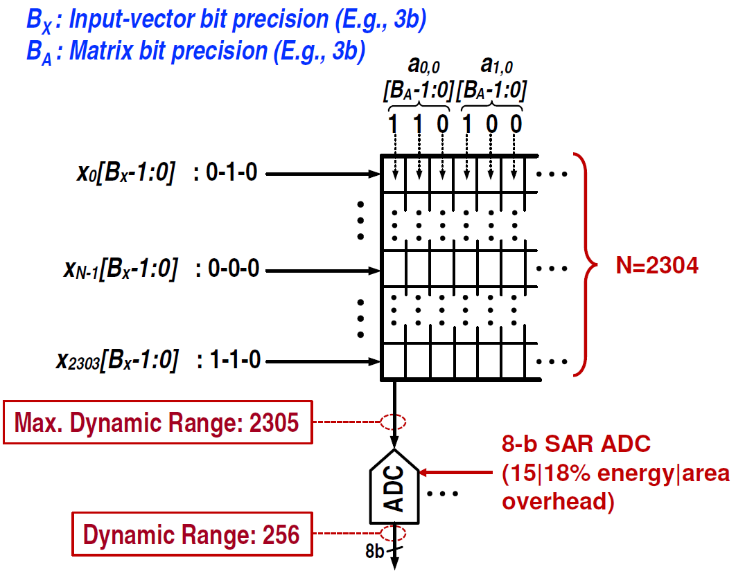
(Click to enlarge. Image courtesy Princeton.)
- They bring in eight inputs at a time, so they time-slice the input vector and do several successive multiplications to get the final result.
- The bit line charge is deposited onto a capacitor; when ready to read, that charge is read out and sent to ADCs for transformation back into the digital domain.
Their basic cell structure is shown here:
(Click to enlarge. Image courtesy Princeton.)
Those capacitors could be cause for die-size concern, but they say they can use the metal above the cell for that. Granted, the full cell is now 80% larger than a standard 6T SRAM cell (even without the capacitor) – already large compared to flash – but they say that they still get a far smaller overall circuit than would be required for a standard digital implementation and without the challenges of a full analog implementation. Because their basic array operations are still digital, they claim much less in the way of susceptibility to noise and variation, meaning that their ADCs can be much simpler and lower power.
(Image courtesy Princeton.)
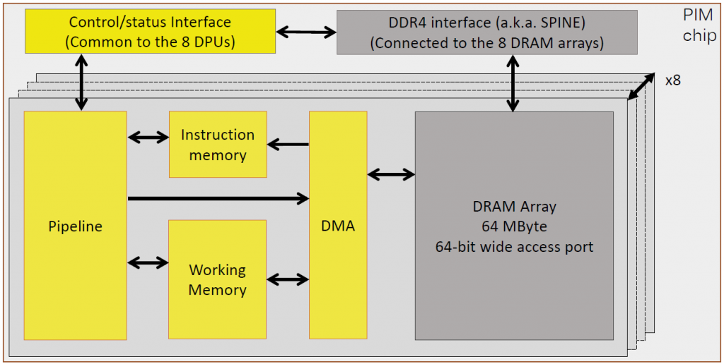
Doing it with… DRAM??
For our final discussion, we turn to a completely different solution from UPMEM, as presented at Hot Chips. From the standpoint of a DRAM chip, this could be considered in-memory computing. But from the standpoint of the memory array, it’s near-memory computing.
The idea is this: instead of using tons of power to grab DRAM contents and somehow muscle them into the CPU or some other computing structure, what if we did the computing on the DRAM die itself?
That’s what UPMEM has done. They’ve built a simple processor on the DRAM die using the DRAM process – something for which the process wasn’t originally intended. They’ve had to make some compromises on the architecture – this isn’t going to compete with a Xeon chip, but then again, it doesn’t need to for what they’re doing. They call the architecture and chip Processing in Memory, or PIM.
(Image courtesy UPMEM)
Instead of bringing the data to the computing, they’re bringing the computing to the data. A routine is offloaded by the main CPU and executes locally in the DRAM chip itself. Then, with no need to move that data anywhere outside the DRAM chip, only the result of the computation needs to travel back to the host system. And, given that ML computation often involves a lot of reduction, that result should be less data that what was used to compute it.
They did this with no changes to the process, although they did need some small changes to the DRAM design itself. A standard form-factor DRAM module will now provide multiple opportunities for distributed computing.
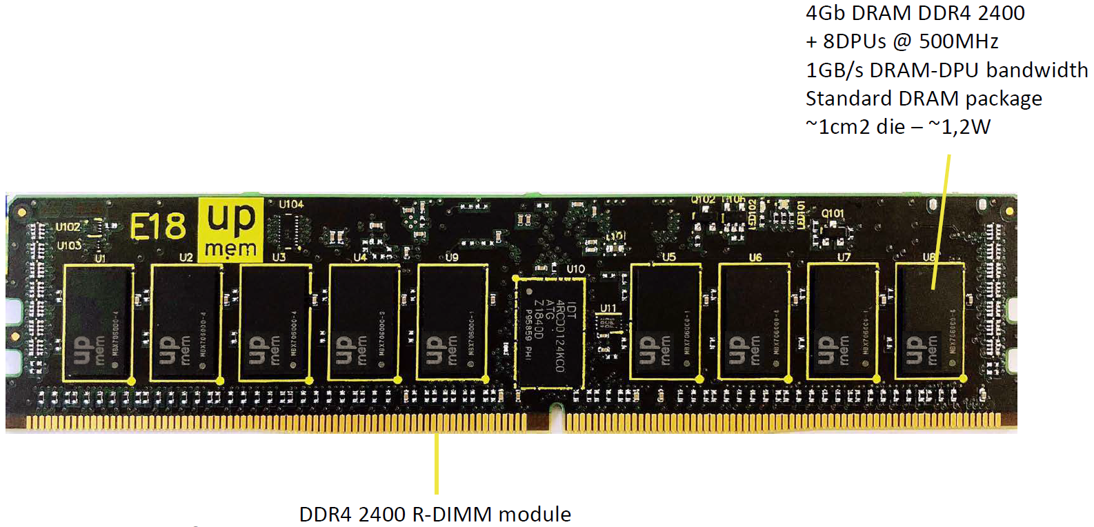
(Click to enlarge. Image courtesy UPMEM)
Is there a downside to this? There is the complication of writing complete programs that leverage this; their tool suite and flow are intended to address this. So, other than being “not the way things are normally done,” I didn’t see any red flags (assuming they’ve executed properly and can supply reliably).
(Click to enlarge. Image courtesy UPMEM)
They expect that the server using the PIM offload will consume twice the energy of a standard server connected to PIM-less DRAM modules. But, with 20x the throughput, it still gives them a 10x energy-efficiency advantage. Another example of “spend more locally to spend less globally.”
They also suggest that this approach can help against side-channel security attacks. This comes from the fact that, what would have been a single contained set of computing threads in the CPU(s) becomes this spray of threads to the DRAMs. You now need to attack all of the DRAMs and somehow figure out which thread is going where in order to make any sense out of the attack data. Their expectation is that this will be a very hard task.
So there you have it. In-memory computing approaches leveraging pretty much any memory technology you can think of. You can find much more detail in the links below.
More info:
Sourcing credit:
Ranga Srinivasan – Business Development Manager, License Marketing, Silicon Storage Technology (SST) a wholly owned subsidiary of Microchip Technology
Pascal Adam – Product Marketing Manager, License Marketing, Silicon Storage Technology (SST) a wholly owned subsidiary of Microchip Technology
Mark Reiten – Vice President, License Marketing, Silicon Storage Technology (SST) a wholly owned subsidiary of Microchip Technology
Mike Henry, Founder and CEO, Mythic
Tim Vehling, SVP Product and Business Development, Mythic
Hongyang Jia, Graduate Student, Princeton University
Fabrice Devaux, CTO and Co-founder, UPMEM
Gilles Hamou, CEO and Co-founder, UPMEM


What do you think about all of these variants on the notion of in-memory computing?