


Memory is memory, right? OK, OK, yeah, there’s different types. DRAM, SRAM, non-volatile (typically NOR and NAND). But, within each family, memory is memory. Right?
Well, maybe not. Micron had a couple of NAND announcements, and the features they highlighted were definitely targeted at specific markets: consumer IoT (CIoT), industrial IoT (IIoT), automotive, and mobile. So – perhaps density aside – why would it matter where the memory is going? Let’s take a walk through the situation to see.
Bulking up NAND
Micron’s first announcement targeted IoT and automotive, although they divide that target market into three subgroups with different needs:
- IIoT
- High reliability
- A wider temperature range
- Security
- Assurance of long-term product availability (since industrial equipment lasts much longer than consumer gadgetry)
- Automotive and mil/aero or other hi-reliability systems
- High reliability
- A wider temperature range – specifically from -40 to 105 °C for automotive
- A “zero-defect” approach, involving specific automotive flows and quality standards.
- CIoT
- Cost
- Opportunities for cost optimization and innovation through small packages
With that in mind, they made some tweaks to their 25-nm planar NAND process to improve the temperature and reliability numbers. They doubled endurance from 60,000 cycles to 120,000 cycles; they also doubled data retention from 5 years to 10 (both at 85 °C).
They’re also claiming the highest performance in this class, at 11 MB/s and 5 MB/s for read and program, respectively.
To be clear, this is SLC NAND. As a quick reminder, “SLC” means “single-level cell,” and it refers to the fact that each memory cell stores a single bit. This is in contrast to MLC (multiple-level cell, where “multiple” = 2) and TLC (three- (or triple-) level cell), which store 2 or 3 bits’ worth of data, respectively.
With all of these, you’re transferring some amount of charge into a holding place. SLC means that there’s a single charge dose, and either it’s there or it’s not, giving you 0 and 1 as possible states. With MLC, you can detect finer gradations, with quarter, half, and three-quarter doses detected. So each cell gives you two bits – double the memory size for the same number of cells. And TLC is finer yet – you can detect eight levels, tripling capacity.
There’s a cost of the increased density of MLC and TLC, of course. Reading these cells at the fine levels we’re talking about is tough, which is why they use error correction circuitry (ECC) to clean up the readout. And the amount of bit redundancy needed for ECC is much higher if you’re trying to do delicate TLC (or even MLC) reads. According to one Micron chart, with 34-nm silicon, SLC ECC requires 4 bits; MLC requires about 20 bits (using my visual interpolation), and TLC requires as many as 60 bits.
For cost-conscious applications, the higher density cells require too much overhead; cost is a reason to stick with SLC.
But there’s another consideration. They’re choosing the 25-nm node, also for cost purposes, and that node requires 8-bit ECC. But they’d also like to be plug-in compatible with other sockets using memories that have 1- or 4-bit ECC.
And this highlights the challenge with ECC: as the process moves, the ECC level changes. Which is kind of a drag, since it means that the technology node can’t be made transparent to the design; the design specifically has to take the ECC level into account.
Of course, the reason for this is that the ECC calculations are typically done in a controller or host; that’s why the ECC level matters. What Micron has done with this release is to provide an option to handle the ECC on-chip so that it becomes transparent.
The small-package requirement is met using the SPI interface (they claim that this is their second-generation SPI offering). The space savings that this enables is made pretty clear by the following figure. The image on the left uses SPI flash; the image on the right uses parallel flash.
(Image courtesy Forward Insights, Report No. FI-NFL-SLC-1014)
Finally, they’ve put security features in the memory to give protections to critical memory contents. (Not all of these are new, of course…) In particular, they list, in order of increasing security:
- Volatile Block Protection allows memory blocks to be locked against programming or erasure. This can survive a power cycle, but can be removed (hence “volatile”).
- Hardware write protection prevents the block protection bits from being changed. This can be changed on the fly.
- While the write protection prevents changes to blocks, Device Lock Tight prevents changes to the lock state (in either direction). Very meta. Once set, it takes a power cycle to remove it.
- Permanent Block Lock: up to 48 blocks can be permanently protected; this can never be changed, even with a power cycle.
- OTP Data Protect turns 10 pages of the memory into one-time programmable (OTP) memory. Once programmed, they can never be erased or changed; this setting can never be changed or undone.
The harder you lock your memory down, the harder it is for someone to monkey with the contents – especially your code. But also, the harder it is to issue code updates to existing code. Where the code is protected, you have to turn to some other unused area of memory for the new code image.
In other words, you’re not patching the existing code; you’re replacing it, and the old code sticks around without doing anything. With the current tendency to release quickly and then fix as you go, you have to think about how many updates you can sustain. If you really want to do frequent updates, then you can’t use the most aggressive security settings.
Going Mobile
Meanwhile, in a separate announcement, Micron launched a new 3D NAND offering for mobile. You might recall that we talked about Micron’s 3D NAND (done jointly with Intel) early this year, and you can get more detail there.
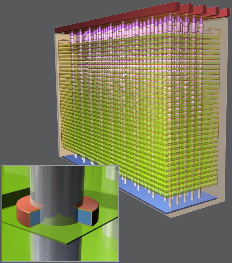
(Image courtesy Micron Technology)
While the mobile announcement focused on the NAND aspects of the package, it turns out that there are nine dice lurking in the package: 4 NAND dice (stacked, although not with TSVs), 4 DRAM dice, and 1 memory controller.
Micron is touting several firsts with respect to mobile memory.
- Their first floating-gate 3D mobile memory
- Their first memory with a UFS NAND interface
- Their first memory with an LPDDR4X DRAM interface.
The underlying NAND die has 8-GB capacity, achieved through MLC technology (two bits per cell), in contrast to the SLC device we just discussed. Micron says it’s the world’s smallest 8-GB die, at 60.217 mm2.
The UFS interface is a newer serial NAND interface that comes as a higher-speed (and fewer-pin-count) option to the older eMMC parallel interface. They’ve achieved so-called Gear 3 performance, which specifies 5.83 Gbps. They have three NAND/DRAM combos, all 32 GB NAND and 3 GB DRAM; two are eMCC, one is UFS. They also have a NAND-only UFS device.
Meanwhile, the LPDDR4X interface, with its lower voltage than LPDDR4, offers up to 20% better power efficiency as compared to LPDDR4. Of the two eMMC devices, one is LPDDR4, the other LPDDR4X.
Product is sampling now to select companies; broad availability is scheduled for Q4 of this year (which is Q2 of their 2017 fiscal year – in case you see Q2 ’17 shown somewhere).
More info:


What do you think of Micron’s IoT and Mobile memory announcements?