


One of the tricky bits when launching a new process is figuring out what the process window is. For anyone new to the concept, the window is the range of variation that’s allowable for a given process parameter. Go outside that range, and a die – or a wafer – or a lot – may fail. It’s best if you can have a wide window, because then you can tolerate lots of variability. If the window is too narrow, then you’re spending all your time trying to thwart that variation and keep the equipment in the straight and narrow.
But, to be clear, there’s the actual window, which you would like to be wide, and then there’s the specified window, which you would like to be… right. If you specify the window to be wider than the actual window allows, then you’re going to have yield problems for those lots processed within the specified window but on the fringes or outside the actual window. On the other hand, if you specify the window to be narrower than it has to be, well, then you’re just being difficult.
So it’s a Goldilocks thing: the specified window has to be just right. Question is, how do you know what “just right” is? Another way of asking the question is, “What’s the actual window?”
That’s a question that Coventor has set out to answer in their latest release of their SEMulator3D tools (version 8.0). To be clear, determining a process window isn’t new; it’s been a thing since processing got started, and it’s not a notion unique to semiconductors. So we’ve been doing it for decades using experiments to figure out where the window edges are.
But that takes a lot of wafers (read “money”) and time (OK, also read “money”). So you try to do enough to get a good bead on the window and launch. But you might not have specified the optimal – i.e., actual – window, but rather one that simply works OK. It’s just that you don’t want to commit the wafers and time to dial it in even better. So you live with what you have.
But the thing with SEMulator3D is that it can do virtual processing of wafers. Millions of wafers, if you want. With that in hand, it raises the possibility of tweaking the specified process window to improve yields. You might widen or narrow it, or you might shift it a bit to move the center, or you might do some of all of the above.
Even with that, though, there are still tons of parameters over the entire processing lifetime of a wafer. Some of those parameters are independent of others, some are correlated with each other, and some are more important than others. So we’re not talking about running all parameters in all possible combinations to optimize things; we’ll be selective. But how to select?
It turns out that SEMulator3D has an Identify Important Parameters feature that can be used based on the results of a comprehensive design of experiments (DoE). Those parameters can then be the focus of further refinement and optimization.
There are a few steps involved in the process. The first is process model calibration, which we’ve discussed before, where you make sure that the process models that SEMulator3D uses are dialed in for correlation with physical measurements. At this point, that could be focused on the parameters identified as important.
Next, you specify a search space. For each parameter, you provide the nominal value and type of distribution – either uniform or normal. If uniform, then you give the width of the distribution; if normal, you give the standard deviation.
The tool then goes off and varies the parameters about the nominal value, according to the distribution info provided. They do a Monte Carlo experiment, which allows them to use thousands, rather than millions, of data points. This ensures a full, unbiased set of results – in contrast to what other experimental designs may generate (where you could even have parameter values making the process fail outright – like having an etch that’s too long and accidentally wipes out a feature).
They then calculate an “inSpec%” for various parameter combination windows. One way of viewing the results is through Univariate Parameter Sensitivity, where they sweep one parameter while keeping the others constant to see how the yield varies. This is done with confidence intervals, which are calculated by the tool from the distribution information you provided. An example is shown below, where the red curve indicates the nominal inSpec% value, and the purple lines indicate the confidence interval.
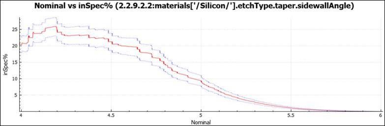
(Image courtesy Coventor)
The data that supports this part of the analysis is generated automatically by the tool. Users can further go in and tweak different parameter values – change nominal, change the distribution, or change the distribution width. The procedure can then be repeated to compare the different results.
During the analysis, Coventor says that they slide a small window around, calculating for each position what percentage would yield. Calling that a “window” is a good mental way of picturing what’s happening, but it reduces the space to two dimensions. They say that their analysis is multivariate, meaning that this is an n-dimensional window: they’re moving all parameters at once.
This helps to deal with the possibility of correlated parameters – ones that aren’t strictly independent, but interact with each other. Change one, and the other changes. That’s another way of saying that they’re not mutually orthogonal. But because they’re including all of the identified parameters in that sweep, those interactions automatically play out in the calculations, so they’ll be reflected correctly in the results.
In some of the examples they give, a slight change in process can result in meaningful yield improvement. In one case involving two SAQP spacer thickness values, changing one spacer thickness nominal value from 13.5 to 13. 4 nm and the other thickness nominal value from 18.8 to 18.9 nm resulted in an inSpec% increase from 69.6% to 74.6% – a significant increase from a tiny change in parameters.
It was done using 1000 different process points. You might say, “OK, that didn’t take millions of wafers; it took 1000. Not so bad…” But here’s the thing: fab operators never try to miss the target nominal values. It’s just a natural thing that happens with equipment, depending on uncontrollable conditions like, did the equipment get a good breakfast that morning? So you can’t simply dial up 1000 different wafers with specific deterministic variations in value. You need lots more wafers to ensure that you populate the entire space adequately.
With the virtual equivalent, you have an ideal process that does exactly what you said, regardless of whether breakfast was full English or a crappy cheap-hotel pastry. You don’t need all of those other points to fill in the space.
So you still spend some time optimizing the process window, and there may be some manual effort involved, but, if everything goes as promised, you’ve got that optimization without the cost and time involved in building actual wafers.
More info:
Sourcing credit:
Bill Egan, Senior Product Manager, Coventor (Lam Research)


What do you think of Coventor’s way of doing semiconductor process window optimization?