

“The hot side stays hot and the cool side stays cool” – McDonald’s pitch for the short-lived McDLT
Ah, the quaint old days, back when you assembled the analog and digital parts of a system out of separate components. The analog side got the analog parts that were made on analog processes, and the digital side got the digital parts made on digital processes. And you somehow hooked them together.
Yeah, that doesn’t work so well in the age of the system-on-chip (SoC). Now you have to host the analog and digital on the same chip using the same process. And, to hear Movellus tell it, when a new SoC is planned, the analog portions get their design starts one to two years ahead of the digital portions – with test chips needed to verify their functionality.
Of course, a big difference between the analog and digital design processes can be summed up in one word: automation. We no longer design anything close to a digital gate (not counting library creation). We write in a programming language for some parts of it and plug in IP for others. Boom: instant billions of gates. OK… maybe not instant, but it must feel like that compared to analog.
With analog, of course, each transistor is lovingly buffed to a high sheen. Yeah, there might be some IP, but because analog has to be tuned for each process node in each fab, you’re unlikely to have a rich assortment of anything above really small components like op amps. Most of the design is done at a really low level. Even something as basic as a current mirror may have to be handled by hand to get it laid out perfectly.
There have been attempts at automation – analog synthesis, if you will – that have failed. It’s easy to blame it on suspicious, conservative expert analog designers who will never trust a tool to do it right (not to mention the tool potentially making their expertise mostly irrelevant and putting their jobs at risk).
But that’s too facile. A big part of it has to be that the automation never really did work well enough. After all, if a tool worked as well as the expert – but tons faster – then, as with any other field, the expert would eventually be obsolete, pushback notwithstanding. And that hasn’t happened. Yes, there are some assist tools, but, ultimately, the designer is still in charge of each transistor.
One approach to solving this is to move the analog/digital boundary closer and closer to the pins, banishing the true analog to the outermost reaches of the realm. DSP tends to pick up the newly digitized functions, but that’s been done only in fits and starts, like the transmitter and receiver work done by Cambridge Consultants that we covered last year. As far as I can tell, this hasn’t taken over manual analog design.
This problem has been ripe for a solution for decades. Literally. So, with an opportunity like that, someone’s always going to be tempted to solve it. It’s just that you have to find new ways that are better than the old ways that didn’t catch on.
So that’s the productivity challenge. But, even if it were more productive, there’s another problem with true analog design: it relies heavily on passives – resistors, capacitors, and inductors. Those don’t come cheap on silicon. And there’s yet another issue: when it comes to full-chip verification, the analog blocks are typically black-boxed because the simulator can’t work with analog. These two issues aren’t affected by automation; even with automated circuits, they’d still be a problem.
Digilog Design
So today we’re here to talk about yet another new approach that’s dramatically different from most prior ways. One that addresses automation, passives, and simulation. This Movellus company has figured out how to implement analog functions using digital design. No, that doesn’t mean doing analog design on a process optimized for digital transistors, and it doesn’t mean converting analog into DSP. It means, literally, doing analog design using the standard digital flow.
In other words, you’re getting analog functions out of digital circuits. For you portmanteau fans, I propose to call it digilog design. Because the circuits are digital, they don’t rely on passives, and the blocks don’t have to be black-boxed; every transistor can (in principle) be verified.
“How can this be possible??” you might wonder. Well, it requires a few ingredients:
- Circuit generators from Movellus
- EDA add-ons for synthesis, place-and-route, power analysis, and static timing analysis
- Three new library cells (which appear to be optional in the figure below) that enable analog concepts like a continuous range of voltages. They’re trying to get those cells into the foundry libraries, although that hasn’t happened yet.
The EDA add-ons are brand-agnostic, so they should work with your favorite tools. And, because this is truly digital, you can include DFT circuits and link the analog functions into the scan chain.
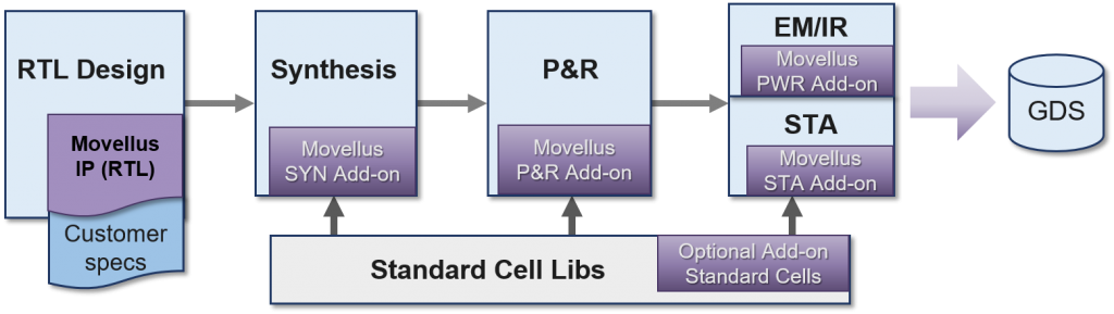
(Image courtesy Movellus)
Of course, one big issue with analog is noise. With true digital signals, you have great noise immunity because subtle perturbations overlaid on your 1s and 0s remain well within the noise margin. Not so with analog. With this digilog thing, they say they have some special tricks that give them good noise immunity.
New Generators
They’ve come out touting their first three digilog circuit generators: ones for phase-locked loops (PLLs), delay-locked loops (DLLs), and low-dropout regulators (LDOs). Using digital gates, they say that the architectures for building these are completely different, looking nothing like their traditional analog counterparts.
There are also bits and pieces of these circuits that will be useful in other circuits. As they go forward with more generators, they say that the process will get easier as they leverage stuff done on the prior ones.
These generators take the parameters a designer wants and spit out a circuit that implements the targeted function tuned to those parameters. Because the generators don’t specify a process node or fab, they’re usable with any set of libraries. The magic then happens with those libraries and with the EDA-tool add-ons.
To be clear, this means that, from a design flow standpoint, you follow the normal digital flow – even for the analog portions. The tool add-ons allow that flow to process the generated circuits just as if the circuits were synthesized from RTL. (OK, actually, presumably they are synthesized from RTL – it’s just that the RTL was created by the generator, not manually.)
And, to be clearer yet, only the PLL generator is available now. The other two will debut in the second half of 2018.
The result is the ability to create circuits in hours (which is machine time, not human time) rather than weeks or more. In fact, if it all pans out, you could envision the analog portions of an SoC starting at the same time as the digital portions – saving one to two years and several test-chip cycles. If that happens, that would be the biggest analog design win in a long time – maybe ever.
More info:


What do you think of Movellus approach to creating analog circuits?