


Did you ever see the Doctor Who episode “Vincent and the Doctor”? This starts with the Doctor and his companion, Amy, visiting a Vincent van Gogh exhibition at the Musée d’Orsay in Paris. When they spot an alien creature in one of Vincent’s paintings, they travel back in time to find out what’s happening and sort things out.
We now regard Vincent as being an artistic genius, but his paintings were largely unappreciated and rejected by critics and the public while he was alive. In fact, we know of only one painting that he sold for sure. Happily, at the end of the episode, the Doctor and Amy bring Vincent to our time and take him to the exhibition of his work. Vincent hears the art curator Dr. Black (played by Bill Nighy) say that he was “the greatest painter of them all” and “one of the greatest men who ever lived.” I don’t mind admitting that this brought a little tear to my eye.
I’ve often thought that if I ever get my own time machine to work (you simply cannot find the spare parts where I live), I’d love to bring Orville and Wilbur Wright to our time. Obviously, I couldn’t take them on a flight (I don’t have the cash to splash, and they wouldn’t have any ID that would work), but we could visit an airport and they could watch today’s planes taking off and landing.
Similarly, I’d love to pick up Philo Farnsworth and John Logie Baird, bring them to my house, give them a cup of tea (or a glass of whiskey), and let them drool over the 65” high-definition color television in our family room.
And, of course, I’d really like to bring John Bardeen and Walter Brattain to our time and show them how their first palm-sized transistor has evolved to power things like smartphones and tablet computers and color televisions (I’m afraid we’d have to leave William Shockley behind because he turned out to be a racist and eugenicist nutter). Similarly, I’d love to show Marcian “Ted” Hoff, Stanley Mazor, Masatoshi Shima, and Federico Faggin how their Intel 4004 microprocessor has grown into today’s awesome processing devices.
Why am I waffling on about all this? I have no idea. I’m sorry, I got carried away. Oh yes, I remember now. I was just thinking about the time when silicon chips reached the 1um process node circa 1984. When we say things like “1nm process,” we’re talking about the size of the smallest structures we can create in or on the silicon chip (this is something of a simplification, but it’s “close enough [to the truth] for government work,” as we might say).
With the introduction of the 1um node, the pundits of the time said this was as low as we could go. They kept on singing the same song without any embarrassment when the 800nm node arrived in 1987, followed by the 600nm node in 1990, the 250nm node in 1996, the 90nm node in 2003, and the 65nm node in 2005.
Personally, I was blown away by the 10nm node in 2016. “Surely this has to be it,” I thought to myself, but no, because this was followed by the 7nm node in 2018, the 5nm node in 2020, and the 3nm node in 2022, with the 2nm node anticipated in 2024. “Oh, my goodness gracious me,” is all I can say.
Well, of course that’s not all I can say, otherwise this would be a bit of a pointless column.
Just when I thought things couldn’t get any more exciting, I found myself chatting with Robert Mears, who is Founder and CTO at Atomera, and Jeff Lewis, who is Senior VP, Business Development and Marketing at Atomera (“Atom Era,” get it?).
From their website we read, “Atomera has created a patented, quantum engineered material called Mears Silicon Technology (MST), which enhances transistors to deliver significantly better performance in today’s electronics. This means your mobile phone will have longer battery life, IoT devices can be made smaller, and web servers will become even more powerful.”
I must admit that I was tempted to add “And it will make your teeth look whiter and your breath sweeter” (in a sarcastic way, you understand). However, after chatting with Robert and Jeff, I wouldn’t be surprised to discover that making our teeth whiter was just one more of MST’s awesome powers.
The fruit of over 15 years of research and development with more than 300 patents granted and pending, MST is a chemical vapor deposition process that allows you to grow an epitaxial layer on your silicon wafer. I was informed that this starts off as a silicon layer, which I found to be a tad underwhelming at first. “So, all we do is add silicon on top of silicon,” I thought, but I hadn’t heard the clever bit yet, which is that they can introduce “puffs of oxygen” into the mix.
“Ah ha! You are adding a layer of silicon dioxide (SiO2),” I said. “No,” they retorted. “What? Then you are adding O2 into the silicon matrix,” I suggested. “No again,” they replied. Although I find it hard to wrap my brain around this, the MST process allows you to introduce a layer of individual oxygen atoms that “sit” on top of the Si-Si bonds in the silicon matrix. Moreover, you can add as many layers as you wish, with different numbers of layers resulting in different properties.
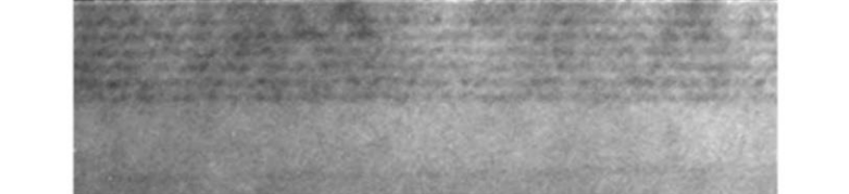
Example results from the MST process (Source: Atomera)
In the image above, for example, the thick light gray band at the bottom is the upper surface of the silicon wafer. The darker and lighter bands above are 1-atom-thick layers of oxygen and silicon, respectively. Read that again! Layers that are only a single atom in thickness! If I were to go back in time and show them this image, I have no doubt that John Bardeen and Walter Brattain would squeal like… well, things that squeal in high-pitched voices.
These quantum-engineered thin films can enhance the power, performance, area, and cost of transistors. Even better, MST is effective across all process nodes and many application areas. For example, it can work its magic with legacy nodes, BCD, Power, analog, and RF-SOI; it can invigorate memory devices such as MRAM and ReRAM; it’s super effective on mainstream planar processes; and it can boost the performance and power efficiency of state-of-the art digital process technologies and advanced nodes like FinFET and Gate-All-Around (GAA)! What’s not to love?
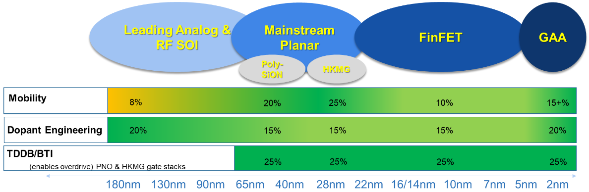
Behold the power of MST (Source: Atomera)
“But what do I have to give up if I employ MST?” You might ask with a furrowed frown. “Not a thing,” I would reply with a sunny smile, “because the benefits of MST are both additive and complementary to other enhancement technologies!”
Take another look at the image above. “What is ‘Dopant Engineering’?” I hear you mutter under your breath.” I know just how you feel. “What is ‘Dopant Engineering’?” I asked Robert and Jeff. I wish I hadn’t because they responded with a barrage of slides that made my head hurt and my eyes water. One of their simpler slide offerings is proffered below.
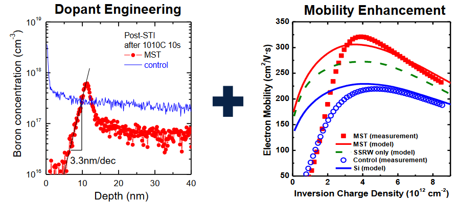
MST enhancements to CMOS devices (Source: SK-Hynix, UC-Berkeley, and Atomera)
The notes accompanying this slide tell us that MST provides a toolbox for both NMOS and PMOS transistors. We also learn that Gm, Idlin, and Idsat are enhanced via 50% lower surface roughness scattering, that gate leakage is reduced 2.7X (HKMG), that precision doping profiles give a >50% lower mismatch with reduced DIBL and GIDL, and that there’s a 10X BTI reliability improvement for PNO and HKMG, higher overdrive, and improved PPAC drivers. Talk about TLAs (three-letter acronyms). Now I know what my family and friends feel like when they are talking to me.
Well, that certainly clears things up, doesn’t it? Of course, if (like me) you don’t have a clue what any of this means, then let me at least summarize things a little. Let’s start with the “Dopant Engineering” graph on the left-hand side. One of the things about adding a doped region to the silicon substrate is that every time you re-heat the silicon in a later step, the dopant atoms continue to permeate deeper into the matrix of the silicon substrate.
The blue “control” line shows what happens without using MST. In this case, the proportion of dopant atoms starts off high at the surface and quickly levels off to be relatively constant from around 2nm to 40nm deep into the silicon substrate. By comparison, the red “trace” shows what happens when MST is employed. In this case, the dopant is essentially non-existent at the surface, and it peaks at around 10nm deep into the silicon. Apparently, process engineers (who rarely even crack a smile) do everything but swoon with joy when they see this curve.
Now let’s turn our attention to the “Mobility Enhancement” graph on the right-hand side. All we really need to know here is that greater mobility is a good thing, and that using MST gives you greater mobility. Case closed!
![]()
Architectural evolution of transistors (Source: Atomera)
In the case of the most advanced transistors, including planar, FinFET, and GAA, MST blocks source/drain dopant diffusion, provides an enhanced punch-through stop layer between the source and the drain, lowers contact resistance, reduces the HKMG stack height, and improves carrier mobility and gate leakage.
As one final point for the moment, in a recent column—Boosting Semiconductor Fab Productivity by up to 20 Percent!—we discussed how the equipment used to fabricate silicon chips is eye-wateringly expensive. So, you’ll be delighted to discover that MST is supported by the major EPI (epitaxy) tool suppliers, which means employing MST doesn’t dramatically change the cost of building a silicon chip.
I fear that I’ve only scratched the surface of all MST has to offer, but delving deeper is beyond my power to describe. On the bright side, the folks at Atomera would like nothing better than for you to call and say, “Can you please explain what on Earth Max was waffling on about.” Of course, if you have any simple questions, then I would be delighted to hear them and answer them myself in the comments below.


The sentence should read across all process nodes not notes.
These quantum-engineered thin films can enhance the power, performance, area, and cost of transistors. Even better, MST is effective across all process notes and many application areas.
Arrggghh — great catch — I just made the change — now I must chastise myself soundly 🙂
As I understand it, Else Kooi (from Philips) had the early epi patents. Just skimmed your Atomera article.
More detail here: https://patents.justia.com/inventor/else-kooi
-JJ
Very interesting — thanks for sharing Jesse — much appreciated — Max