

Metrology is the scientific study of measurement. The ability to measure things helps in locating and identifying problems and weak spots in production lines and processes. I was just introduced to a new molecular sensor for semiconductor metrology that may be poised to take the chip fabrication process by storm, but first…
When we look around, it’s easy to be awed by all of the amazing technology that surrounds us. I know I am. But I also know that we are prone to making errors (when I say “we,” I’m referring to the human race — other people — not myself, you understand). Over the centuries, we’ve dropped the metaphorical ball on numerous occasions.
Take the Greek mathematician and engineer Hero of Alexandria (10 AD to 70 AD), for example. Hailing from Alexandria in Roman Egypt (hence his moniker; his ethnicity may have been either Greek or Hellenized Egyptian), Hero is considered to be one of the greatest experimenters of antiquity.
In addition to inventing the first coin-operated vending machine (when a coin was introduced via a slot on the top of the machine, a set amount of holy water was dispensed), Hero also created the first-recorded steam engine. As the Wikipedia tells us:
“Hero described the construction of the aeolipile (a version of which is known as Hero’s engine) which was a rocket-like reaction engine and the first-recorded steam engine (although Vitruvius mentioned the aeolipile in De Architectura some 100 years earlier than Hero). It was described almost two millennia before the industrial revolution.”
Today, Hero’s engine may — at first glance — seem somewhat simple, but there’s actually a lot going on here. Quite apart from anything else, this mechanism is the first known artificially constructed device to transform thermal energy into rotary motion. Consider the illustration below. Heating the water causes it to turn into steam, which expands and occupies a much larger volume. As described by the Venturi effect, which was published by Italian physicist Giovanni Battista Venturi in 1797, when the expanding steam meets the constrictions at the ends of the pipes, in order for the total flow rate to remain the same, its molecules speed up in the constricted region, thereby producing thrust like a rocket engine. As we know from Newton’s third law, every action has an equal and opposite reaction, which — in this case — results in the vessel spinning.
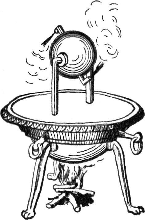
Hero’s Engine
(Image source: The 1876 edition of Knight’s American Mechanical Dictionary)
Hero had already created a wind-powered organ. He was just one small conceptual leap away from creating a real steam engine that performed useful work. Right off the bat, this could have been employed to pump water. How about adding steam-powered propellers to Roman warships? Is it really too much of a stretch to envision steam-powered locomotives barreling around a railway system spanning the Roman Empire? The old proverb saying, “All roads lead to Rome,” might have ended up as “All trains lead to Rome (have you checked the schedule?).” Meanwhile, legions of Roman centurions would have had far fewer problems with their feet, while many other groups of people would have had far more problems with legions of Roman centurions.
It’s not hyperbole to say that this could have radically changed history. The Roman Empire might never have fallen, the Dark Ages might have been a lot lighter, and all the technologies we enjoy today might have been invented far sooner.
Now, you might be tempted to proclaim, “But they couldn’t achieve the necessary precision back in those days,” in which case I would beg to differ. Have you read The Perfectionists: How Precision Engineers Created the Modern World by Simon Winchester? If not, you’ve missed a treat. According to this tome, the gap between the piston and the cylinder on early steam engines circa the 1750s was as wide as an English shilling coin was thick (say 5/64” or 2 mm). As an aside, the shilling was first minted in the reign of Henry VII (1485-1509), at which time it was known as a testoon, but we digress.
The point is that rudimentary steam engines can function without extreme precision, although being able to build the mechanical parts to greater tolerances certainly increases their efficiency. More to the point, engineers from antiquity were capable of achieving extraordinary levels of precision if they set their minds to it. I offer as evidence the Antikythera Mechanism, which is thought to have been constructed by Greek scientists sometime between 205 BC and 87 BC.
This artefact was among wreckage retrieved from a shipwreck off the coast of the Greek island Antikythera in 1901. It is a hand-powered orrery that was used to predict astronomical positions and eclipses decades in advance, and that has been described as the oldest example of an analogue computer.
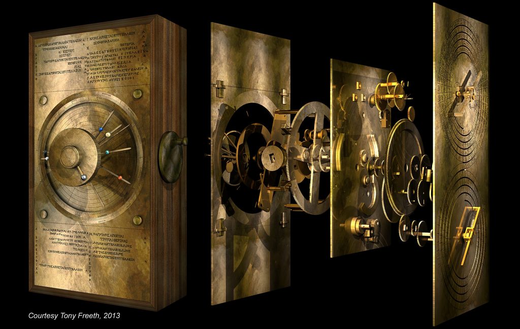
Digital reconstruction of the Antikythera Mechanism
(Image source: Tony Freeth, 2013)
All I’m saying is that, if the ancients could achieve the precision required to construct the Antikythera Mechanism circa 100 BC, then they certainly had the capability to create a rudimentary steam engine circa 50 AD.
I could waffle on about this concept of dropping the ball for hours. We (again, other people, not your humble narrator) have missed many opportunities with regard to inventing things like mechanical computers, vacuum tubes, transistors, and light-emitting diodes (LEDs). In hindsight — which is, of course, the only exact science — we could have created all of these devices years before they eventually saw the light of day (or replaced it, in the case of LEDs).
I was just about to say that, on a somewhat related note, I have a friend who is in the process of creating a fully electronic computer based only on technologies that were available at the fin de siècle (more specifically, technologies that were present in the year 1900 — I fear he’s watched the 1960 version of The Time Machine movie one too many times), but then I ran into a problem relating to what we mean by the term “electronics.” Some people say that “electrical circuits” contain only “passive” components like resistors, capacitors, and inductors, all used in conjunction with things like wires and switches that themselves exhibit resistive, capacitive, and inductive characteristics. These people would also say that – in addition to these passive elements — “electronic circuits” also contain “active” components like transistors.
I also seem to remember hearing that electronic components are those that have the ability to perform amplification, like vacuum tubes and transistors. But, from one point of view, a relay could be employed to “amplify” a voltage or current (i.e., generate a larger output from a smaller input) and that’s an electromechanical device.
I just read a post on Stack Exchange that said, “Electronics refers to technology that works by controlling the motion of electrons in ways that go beyond electrodynamic properties like voltage and current […] Typically, if something uses electricity merely as energy, it is electrical, while if it uses electricity as the medium for manipulating information, it is almost surely electronic.” I also saw a column on Bright Knowledge that said, “The main difference between electrical and electronic circuits is that electrical circuits have no decision making (processing) capability, whilst electronic circuits do.”
Returning to my friend’s creation — this involves building a computer using logic gates and registers formed from cunning combinations of small neon tubes and light-dependent resistors (LDRs). Even the master clock generator is implemented as a ring oscillator that’s formed from these components. So, you tell me — when he finishes this beast, will it be an electrical computer or an electronic computer?
Once again, I fear, we’ve wandered off into the weeds (you really should work harder to restrain me). Returning to the concept of accuracy, the construction of today’s integrated circuits (commonly known as “silicon chips”) requires one of the most exacting production processes ever developed by humankind. Achieving the high levels of accuracy and precision demanded by the semiconductor manufacturing process requires state-of-the-art metrology.
Before we proceed to the point of this column (yes, of course there’s a point), let’s briefly set the scene. The process of creating silicon chips begins with the growing of a single crystal of pure silicon in the form of a cylinder with a diameter that can be anywhere up to 300 mm. The cylinder is cut into paper-thin slices called wafers, which are approximately 0.2 mm thick. (Just this step on its own boggles my mind. How on Earth do they manage to do this?) Next, we build layer after layer on top of the wafer. In some cases, we create an insulating oxide layer, etch holes in it, and dope the silicon with various gases at high temperatures. In other cases, some sort of vapor deposition is used to deposit a layer of metallization, which we then etch to leave tracks.
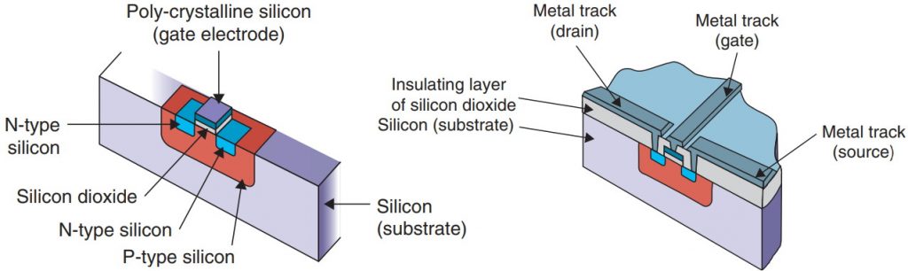
A very simplified cutaway view of a single transistor in the middle of a silicon chip (Image source: Bebop to the Boolean Boogie).
There can be multiple layers of tracks, each separated by layers of insulator and connected by small metallic columns called vias. Creating each layer requires multiple steps. In fact, creating the entire chip can require hundreds and hundreds of steps, each involving varying combinations of high temperatures, solvents, plasmas, and all sorts of noxious (oftentimes poisonous) materials. (If you are interested in learning more, I discuss this process in excruciating detail in my book Bebop to the Boolean Boogie.)
Next, let’s consider what we might find in a semiconductor fabrication facility, which is referred to as a “fab” or a “foundry” for short. A fab may contain say 10 “corridors,” and a typical corridor may comprise 40 “mainframes.” Each mainframe has some number of cassettes that store the wafers in an inert atmosphere (i.e., a noble gas). Also, each mainframe is in charge of performing a group of tasks that go together to form a layer, like depositing an oxide layer, depositing a layer of resist, imaging the resist, removing the unwanted resist, etching the oxide layer, and so forth. While under vacuum, the wafers are automatically conveyed from an incoming cassette to the first chamber, from chamber to chamber, and from the last chamber to an outgoing cassette, where each chamber handles one step in the process. Automation is used to transport the cassettes from mainframe to mainframe.
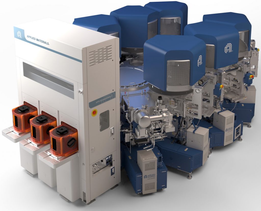
Applied Materials’ Endura Clover mainframe (gray) with cassettes (orange) and a collection of wafer processing chambers (blue)
(Image source: Applied Materials, Inc.)
When it comes to throughput, there can be a huge process variance from step-to-step, with some steps running at only five wafers per hour and others running at 200 wafers per hour. In this case, multiple machines may be run in parallel to address the slower steps. The whole scheduling process is so complex that people have written PhD dissertations on the topic of efficiently organizing the little rascals.
This is where things start to get interesting (maybe I should say “even more interesting”). Until now, performing in-situ metrology on a chamber-by-chamber basis has not been common; one might even go so far as to say unknown. In addition to the fact that devices capable of performing metrology for semiconductor processes are horrendously expensive, they typically haven’t been able to handle the corrosive gasses and condensate particles that abound in these processes and that can damage their sensors. As a result, metrology is oftentimes performed at the end of the process, by which time something that started messing up earlier has had the time to get really messed up.
Also, these things are really variable. Chambers need to be cleaned frequently, but not all chambers need to be cleaned at the same rate. Even two chambers sitting side-by-side performing exactly the same process step may have different cleaning requirements, depending on “stuff.” Over-cleaning a chamber can be as bad, or worse, than under-cleaning one, because the process of continuing to clean an already clean chamber can cause damage to that chamber.
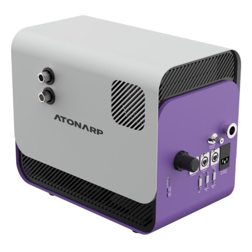
All of which leads me to the fact that I recently had occasion to converse with the chaps and chapesses at Atonarp. These little rapscallions have created a new molecular sensor for semiconductor metrology called the Aston.
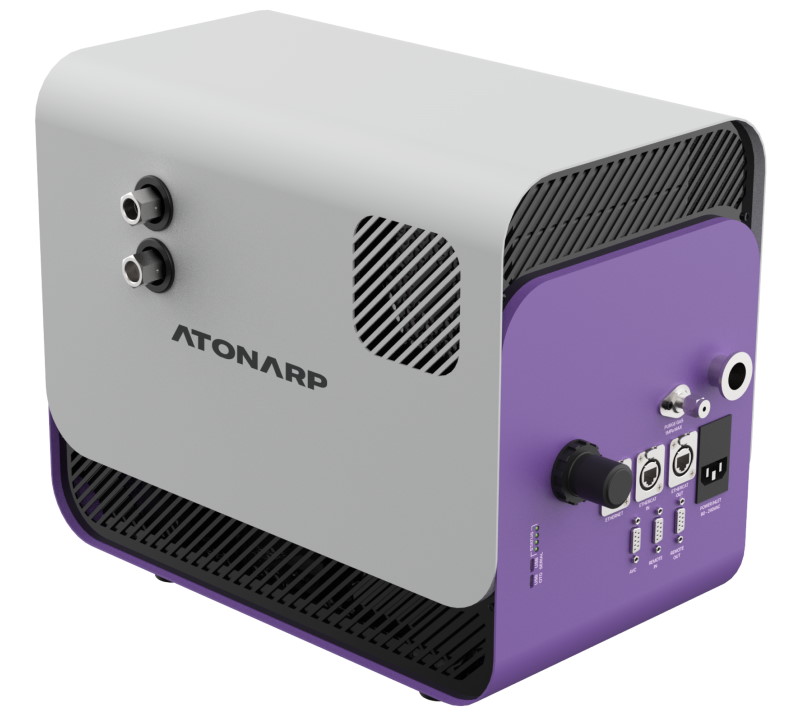
The Aston molecular sensor for semiconductor metrology
(Image source: Atonarp)
In addition to being unaffected by corrosive gasses and condensate particles, this bodacious beauty is small enough (297 mm wide, 400 mm long, 341 mm tall) and affordable enough that the folks creating silicon chips can opt to have one associated with each chamber on each mainframe in each corridor in each fab.
The versatile Aston is a robust single instrument that can replace multiple legacy tools. More importantly, having in-situ metrology provides real-time, chemically specific, and actional information. This information can be employed by advanced data analytics to support autonomous process control, thereby resulting in maximized throughput and increased yield.
Just how big a deal is this? Well, I was just chatting with industry analyst Risto Puhakka, who is President of VLSIresearch. Risto was kind enough to share myriad nuggets of knowledge with me. One thing he said that really struck a chord was: “Even a 1% improvement in yield can equate to hundreds of millions or billions of dollars in market value.”
Ah, now I see why the folks at Atonarp are so excited about the possibilities afforded by their Aston molecular sensor. As always, I’m amazed and awed by everything I learn about the making of the silicon chips that power our modern world. How about you? Do you have any thoughts you’d care to share?


