


We’ve engaged in a decades-long battle to reduce the area footprint of integrated circuits in an attempt to put more faster stuff on one die and sell it for less money. The much-ballyhooed end of Moore’s Law (whether or not you believe that) has spurred much searching for ways around this endless loop. Wait… we’re already going around the loop. How about ways out of the loop?
One of those ways is to escape the tyranny of area by going vertical instead. Yeah, I know, there’s lots of going vertical, what with finFETs and multi-die packaging and whatnot, so let’s get specific: here we’re talking stacking circuits on top of circuits. We’re paving the way from our historical PBJ sandwich – one layer of each ingredient – to a veritable Dagwood sandwich with multiple layers and, perhaps, some unusual ingredients.
We look at two papers from last fall’s IEDM conference. One stacks transistors; the other stacks entire memory cells. And their approaches are very different. But they have both found their way over one important barrier: that of processing temperature. There are lots of high-temp steps in a normal process flow, but what happens if you repeat those steps on multiple layers? That carefully-controlled implant activation might get overactive, throwing its profile completely off. Watching metal melt and ooze out of this sandwich wouldn’t be nearly as appetizing as watching cheese ooze out of a real one. Just to mention a couple things.
There’s one other potential bugaboo that has not been addressed by these projects: that of figuring out how to get the heat from lower layers out. Presumably, that will be a further investigative work by these or other teams. All of that said, let’s dig in.
Stacked FinFETs
The first paper comes from a team from Imec. In it, they place a layer of transistors above an existing, normally processed layer of devices. They skirt the temperature challenge by starting with two different wafers. The first one is processed as normal through deposition of local interconnect. The second wafer is then prepared up to the point of having a silicon layer that’s been pre-implanted so that no further implant or activation is required.
At that point, the second wafer is bonded to the first wafer, and formation of the top-layer finFETs commences. The remaining steps require no more than 525 °C.
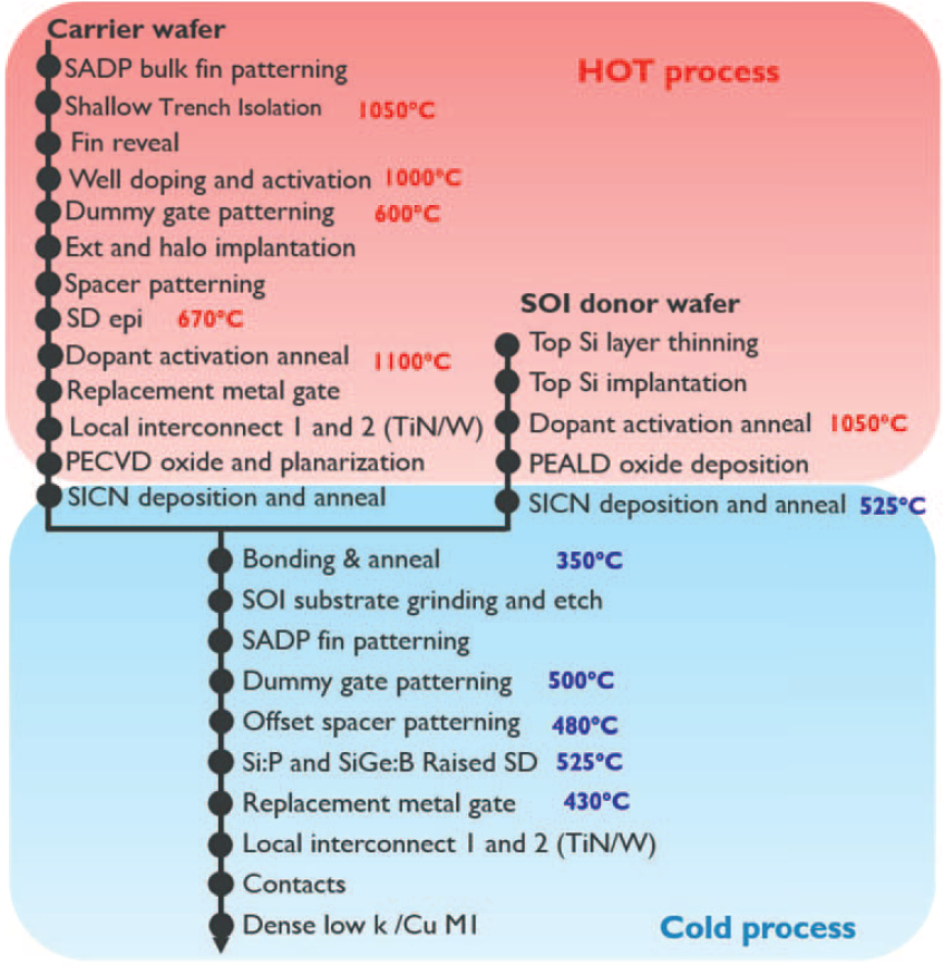
(Image courtesy IEDM; image credit research team)
The top transistors are junctionless, which deserves a moment of explanation. Most transistors have a channel between source and drain, and the interface between source/channel and drain/channel is a PN junction. In order to achieve better short-channel effect and other behaviors, work is being done on so-called junctionless transistors. The most common implementation seems to be using nano-wires. Those nano-wires are heavily doped so that they conduct well and can provide good drive current. The gate is then wrapped around the nano-wire at what becomes an electrical pinch-point. When the OFF voltage is applied to the gate, it cuts off conduction. No junctions involved.
The reason nano-wires are typically used is that this works only if you have a small channel cross-section so that you can control the whole thing. If you have a big chunk of silicon, then that wrapped gate will affect only the outsides of that chunk. This particular paper uses a finFET instead of a nano-wire; presumably it’s small enough for good gate control.
Another critical aspect of this is the ability to align the patterning on the top layer above critical features on the bottom layer. No patterning is done on the top layer until that silicon has been bonded. So the trick here is to align that first patterning layer with the top patterned layer on the bottom wafer. They did this using a 193i stepper, but they found that the most effective alignment could be done with red or infrared (near or far) light.
They also messed with the gate stack to see what would work best. They compared TiN/HfO2, TiN/TiAl/TiN/HfO2, and TiN/HfO2/LaSiOx. That last one brought a couple of benefits, including better bias temperature instability (BTI – negative for p-channel, positive for n-channel).
So how did it go? Well, they created devices on the top with 40-nm fin height, 10-nm fin width, 24-30-nm gate length, and 45-nm fin pitch. They compared their low-temp top layer with a similar set of transistors processed with the normal high-temp steps in order to see what’s being sacrificed at lower temperatures. They found:
- Similar control of short-channel effect;
- For low-power applications, the low-temp version had similar or better on-state current;
And for high-power apps, the low-temp version showed 25% lower on-state current, with one exception: the version with the LaSiOx in the gate stack had only 10% lower current, another of the benefits of that stack.
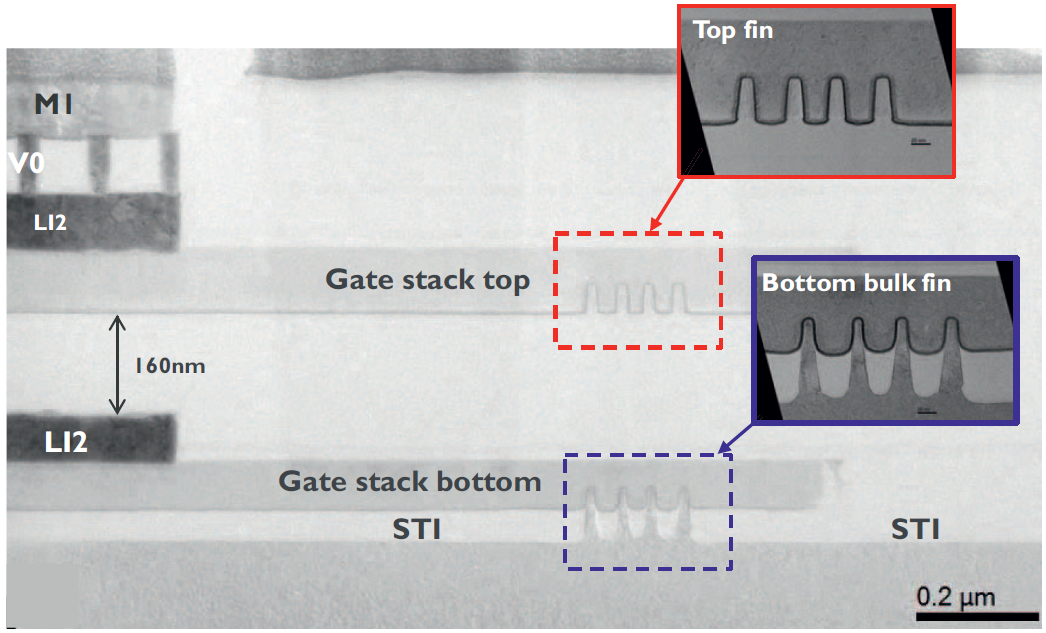
(Image courtesy IEDM; image credit research team)
The only thing that feels to me like something of a gotcha here is that the top transistors are solely n-channel, meaning you couldn’t do CMOS on the top layer. At first it occurred to me that, by patterning the second wafer before bonding and doing a second implant, you could have both n-channel and p-channel on that layer. But there’s a challenge there: part of the idea of this approach is that patterning starts after wafer bonding to improve alignment of the two layers. There’s no need for super-accurate placement when doing the bonding.
Having both transistor types on top, however, would mean patterning for the implants before bonding. That would mean precise aligning during placement of that new layer atop the old layer – the kind of alignment precision that’s not required the way they’re doing it.
I sent a question on this to them and got confirmation. As it is, you can use this for something like RF over logic. CMOS on top would require “… separate implantations for blossom and pumps … followed by aligned bonding,” according to researcher Anne Vandooren.
Stacked RRAM Cells
We completely switch gears for our next paper, done by a team from Stanford Univ. and Soochow Univ. As a reminder, we’re stacking memory cells here, not just transistors. And the entire stacking process is completed at temperatures no greater than 150 °C. (Presumably, a processed base wafer would use normal temperatures prior to stacking the memory.)
Their memory cell is an analog-capable RRAM cell for possible use in neuromorphic designs. Their building process worked for the experiments, but it’s not specifically suited to high-volume production; at the end, they posit that the process can be adapted using standard industrial practices.
They’re using a 1T1R (one transistor, one resistor) cell. The resistor – which is the memory element – is made of hexagonal boron nitride (hBN), with a Ti top electrode. Boron vacancies, along with Ti ion diffusion, are what establish the memory mechanism, building one or more filaments to conduct through the variable resistor. The hBN is very thin, consisting of only a few atomic layers.
The select transistor is yet another surprise: it’s made of a monolayer of MoS2. Yup: just one atomic – er, molecular – layer thick. Both the hBN and the transistor layer are built in a similar way: by growing them on a different substrate and then transferring them to the target wafer. The hBN is grown over copper; the MoS2is grown over silicon; the process is shown below.
![]()
(Image courtesy IEDM; image credit research team)
This is the bit that seems dodgy for full production, so a different approach will be required once (if) this comes out of the experimental stage.
The resulting memory stack looks something like the following, although they intentionally did something to avoid having to mess with the topology of the underlying wafer: they moved the top cell away from the bottom cell by about 1 mm, as indicated in the drawing (where the top cell is to the right of, rather than above, the bottom cell).
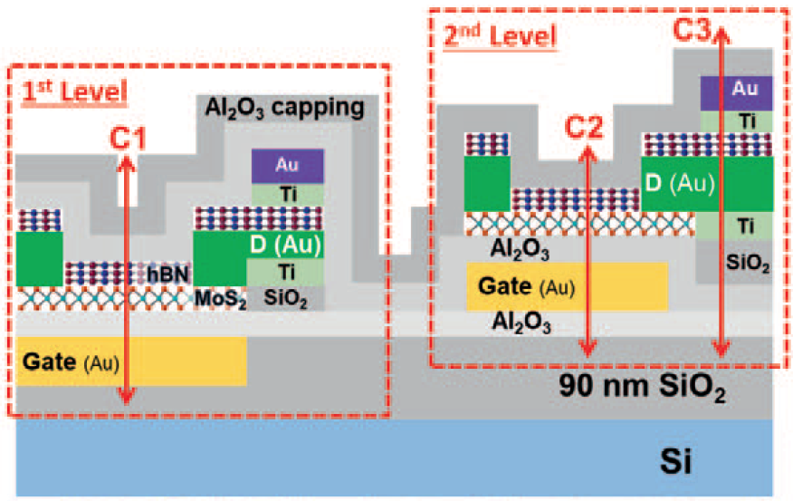
(Image courtesy IEDM; image credit research team)
There’s one possible gotcha here as well, which we talked about last week when discussing RRAM for in-memory computing in neuromorphic designs – an application for which this is also targeted. And that’s the RRAM reliability – or perhaps, better said, the variability issue. As in, do we need ECC for this cell in the manner that it was reported to be needed for other RRAM approaches? If so, then we need to deal with that gate-level burden here. I’ve also sent a question about this; if I get a response, I’ll update.
Of course, I’ve omitted lots of detail; you can get it in the IEDM proceedings.
More info:
Van Dooren et al, “First Demonstration of 3D stacked Finfets at a 45nm fin pitch and 110nm gate pitch technology on 300mm wafers,” IEDM 2018
Wang et al, “3D Monolithic Stacked 1T1R cells using Monolayer MoS2 FET and hBN RRAM Fabricated at Low (150C) Temperature,” IEDM 2018


What do you think of these circuit-stacking ideas from IEDM?
Must incorporate, at least consider, thermal layers; else will remain curiosities.