

What comes after 3D? Going vertical is some folks’ answer to what they perceive as the limitations of planar transistors, but presumably FinFETs will find their finish sometime in the future, so what then? Yet another dimension? (I joke, but these days, nothing would surprise me…)
I saw Prof. Chenming Hu, of FinFET fame, talk at the isQED conference earlier this year. And while he did, of course, talk about his best-known 3D baby, he also discussed work they’re doing beyond the FinFET. And the direction they’re looking is… planar. What’s old is new.
But we’re talking thin. Ultra-thin. He said that, for thin-body FETs, the thickness needs to be less than one third of the gate length. If you’re talking about a 5-nm gate, that means 1-2 atomic layers. You can’t get much thinner than that.
But here’s the thing: we’ve been used to transistors that, more or less, are made out of sand. The sorts of materials used in the gate have had to get more exotic, meaning that there are all kinds of other seed layers and barrier layers and all kinds of stuff that gets lost in the simple gate-stack diagrams, but for the working part of the transistor, we’ve still got simple silicon and its oxide. You can actually contemplate explaining some of this stuff to your kids.
We’ve also looked in the past at other slightly more exotic materials – III/V and SiC and GaN, but they somehow still feel comfortable. Well, get ready to come out of your comfort zone. If there’s anything to be said about the leading edge of semiconductor technology, it’s that we’re going to be designing materials to do exactly what needs to be done. And the materials we’ll talk about today are not the stuff of your everyday integrated circuit. How often have you run into selenium? How many times have you tried to pronounce “molybdenum” after a quaff or two?
Granted, at these sorts of thicknesses, graphene has been something of a popular darling. But it’s got that pesky missing bandgap thing going that pretty much precludes its use for digital logic. Instead, a couple of new materials have been proposed, one of which is in Prof. Hu’s camp, the other not (or… perhaps so, per late-breaking news below). Prof. Hu is looking at WSe2 transistors for p-FETs; a Samsung team has been looking at MoS2 for n-FETs. It’s not at all clear if they’ll ever cohabitate on the same chip – heck, it’s not even clear whether they’ll even make it to production.
But the kinds of issues and considerations being worked on both of these are interesting and somewhat mind-boggling, so we’ll take them one at a time. As a reminder, the goal of any of these devices is high mobility (let’s say over 100 cm2/Vs), a high Ion/Ioff ratio, and a subthreshold slope (SS) as close as possible to 60 mV/dec.
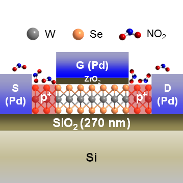
WSe2 has an energy gap of about 1.2 eV and has good surface roughness characteristics (since surface messiness – dangling bonds and whatnot – at this thickness can kill mobility), but early work didn’t look promising. It was ambipolar, with an on/off ratio something less than 10 – not nearly enough to use for a switch. They also had trouble making an ohmic contact with the WSe2 (or with any high-bandgap materials).
The on/off ratio was thought to be due to the fact that they used bulk WSe2 and that leakage through the bulk was the problem. So they effectively chipped off a very thin layer – the word they would use is “exfoliated,” and yes, they were able to peel off a single atomic layer… the concept of which kind of stuns me – and placed that on a SiO2 background.
To deal with the contacts, they picked Pd for its high work function and then doped it heavily with holes. They did this using NO2*, which gets “chemisorbed” into the Pd. From a manufacturing standpoint, they could build the WSe2 channel, cover it with the gate (they used ZrO2), leaving only the ends of the WSe2 exposed where the contacts would be. They could then expose the whole thing to NO2, which would interact only at the ends.
The result: mobility was excellent at 250 cm2/Vs; SS was essentially perfect at 60 mV/dec; and the on/off ratio was over 106. And the contact was ohmic.
In motivating the need for a p-FET, this paper pointed to the promise of a MoS2 n-FET, and so I poked around looking for that. I couldn’t find much widely-available information for either of these technologies, but I was able to track down a paper that details work done on MoS2 transistors by Samsung.
This n-FET side of things isn’t as “clean.” Bulk MoS2 has an indirect bandgap of 1.3 eV, but it turns out that single-layer MoS2 has a direct bandgap of 1.8 eV. Formed over SiO2 with a HfO2 gate, an on/off ratio of 108 was achieved, with a SS of around 70 mV/dec and mobility of around 200 cm2/Vs.
But a Samsung team, in a paper by Kim et al, suggested that laying down the MoS2 and then building a high-? gate over it would be really hard to do commercially. They also point out that multi-layer MoS2 has about three times the density of states of single-layer MoS2, which can boost the current-carrying capacity of the device.
Now, it’s not explicitly clear how many layers are implied by “multi.” The thicknesses they used were 20-80 nm, and from what I can surmise, this would be some tens of atomic layers. So it’s much more than one, but it’s not a lot. Based on Prof. Hu’s rule for gate lengths, however, this would suggest a very long gate… They didn’t report the gate length (that I noticed, anyway), but the Al2O3 backgate thickness was ~50 nm, so presumably we’re not talking about a 5-nm gate (or else that would be one heck of an aspect ratio).
And yes, they got their MoS2 sample through exfoliation. Obviously these teams have that process down.
The performance of this device wasn’t quite as good as the WeS2 or the single-layer MoS2 device, but it had mobility of over 100 cm2/Vs, SS of around 70-80 mV/dec, and an on/off ratio of 106; not bad.
Just as I was about to put this whole topic to bed, I learned that there has been even more recent work by the Berkeley team working with both WSe2 and MoS2. In this case, K was used as the dopant, and not only was an n-type MoS2 device created, but, for the first time, an n-type WSe2 device with mobility of about 110 cm2/Vs was demonstrated. The usual contact issues were addressed, with Ni being used for the MoS2 device and Au for the WSe2 device. They did work with both single-layer and few-layer materials; one obvious conclusion is that the results are very interesting, but more study is needed.
All of which reinforces that this is all very early work and nowhere near consideration for actual adoption (even if issues of commercial production are being incorporated into the thinking). (I can’t help but picture low-cost workers in faraway factories with hammers and chisels, busily exfoliating exotic materials to put into a future phone.)
And I frankly don’t know if we’ll hear about these again, in a year or in five years. But it’s a flavor of what’s happening in some far-flung labs, and whatever we end up doing when we exhaust our FinFETs will reflect this kind of thinking. And it will get yet harder to explain this stuff to our kids.
*No, calm down… not N2O… sorry…
More info:
Subsequent Berkeley n-FET work
Image courtesy Ali Javey, UC Berkeley


Tungsten and selenium and molybdenum and sulfur figure in some new transistors. What other exotic ideas have you seen for the post-silicon era?