


We got away with lax discipline for a long time. Like an out-of-control classroom, we had kids at the front of the class paying attention, while, as you got towards the back, kids were passing notes, tossing spitwads, flying paper planes, and even simply leaving class. The only discipline was imposed from the front; the back and the sides of the room had no enforcement mechanism.
We’re talking, of course, about planar transistors. The gate touched one edge of the channel – the top edge – and that was it. It was enough to get the job done, but electrons farther away from that top edge just didn’t feel the need to obey the gate as much as we might have liked. It worked well enough at the time, but it wasn’t a way forward.
Finagling
So we got our control freak on and figured out how to control three out of four edges of the channel. (Yes, as a three-dimensional object, the roughly right rectangular parallelepiped that is the channel has six faces; we’re discussing the cross section, conveniently ignoring the third dimension.) And so the finFET was born.
![]()
OK, so the top edge of a finFET doesn’t amount to much, what with the sides being angled up. But still, you get to control almost everything except the bottom (which, admittedly, is wider than the top). Is this enough to move forward? Well, yes, for a couple more nodes. But beyond that? Apparently not, since the lifetime of the finFET would appear to be finite.
If we want to exert maximal control, that means we want all four edges of the cross section of the channel. Fair enough. We also want decent current for performance. So, if we maintain the channel as this rectangular thingy (in cross section), then we’ll need it to be relatively thick. But there’s a problem with that, and we’re going to rapidly shift analogies, with apologies for any whiplash induced in the process.
Border Control
If you want to wield mad dictatorial power over a rectangular region, you can set up guard towers and razor wire and barriers and moats all around the rectangle. And anyone near that edge will cower in fear (if not respect), knowing that failure to comply can have grave consequences (literally). But if the rectangle is too large, well, you get a few 10s of miles into the interior, and you can’t see the border, and you can’t hear the megaphones preaching propaganda, and you can almost pretend that there really isn’t any consequence to simply doing what you want. Control wanes towards the middle.
So if you’re really serious about that control, you have to break the single rectangle up into multiples, each with its edges and barriers and heavy-handed discipline so that no one is too far from any edge. It’s no longer possible to escape control.

Nano-Whaaat?
OK, so, conceptually, this has been proposed as the next step for our transistors. But there are two specific practical variations on this concept. One uses nano-wires, the other uses nano-sheets. Of course, our territorial split-up figure above shows an array of 9 resulting regions; this isn’t how folks are implementing it in real life. With an eye towards saving die area, the best way to iterate such a shape would be vertically rather than horizontally. So nano-wires and nano-sheets would be stacked, with intervening gate material that surrounds each nano-wire or nano-sheet. Which is also referred to as gate all around (GAA).
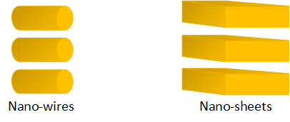
These – especially the nanosheet version – may look like less-trapezoidal finFETs on their sides, but there’s a critical difference. With finFETs, if you need more current, you need to iterate multiple finFETs, meaning that you can’t vary the current capacity continuously: it’s discretized. You can’t have a partial finFET. With nano-sheets, on the other hand, you can vary the capacity continuously by adjusting the width of the sheet through patterning – because it’s horizontal instead of vertical. So this gets us away from this disliked-but-tolerated challenge of finFETs.
That, then, brings us to the next question: nano-wires or nano-sheets? Well, with nano-wires, you don’t get the channel-width knob to turn. Nano-wires offer less current – unless you have multiple stacks, which gets us back to the discrete current-level issue. Nano-sheets can provide more current as well as having that adjustment knob. That said, if you have enough current in the nano-wire version, it takes less area than a nano-sheet.
Whichever one you choose, however, they all look radically different from anything we do today, and so we might expect such a structure to be built using a very different process from what we use now. And, that being the case, you’d expect us to push it off as far into the future as possible.
One of the bigger challenges with nano-sheets is the etch required to separate the channels. They’re built by alternately layering a sacrificial material and Si. The sacrificial stuff is then selectively etched away. But such an etch requires the ability to etch laterally under the nano-sheets to clear that space completely. That’s a challenging aspect of this idea.
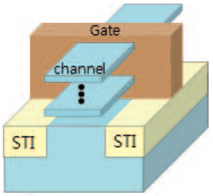
Well, this is all a long way of getting us into a paper presented by Samsung at last December’s IEDM conference. It targets the 3-nm node, so, yes, it’s way out there. But the goal of their project was to maintain as much compatibility as possible with incumbent CMOS processes. They use nano-sheets, and they call their finished structure a multi-bridge channel FET, or MBCFET. They use SiGe as the sacrificial material between the nano-sheets. Unlike other processes, the channel is not deposited and etched; it’s grown epitaxially, providing greater uniformity.
(Image courtesy IEDM, image credit Samsung)
Results included:
- A claimed 90% compatibility with prior processes;
- A subthreshold swing of 65 and 67 mV/decade for N-type and P-type transistors, respectively;
- Three different thresholds, implemented by using three different work function metals;
- Reliability that is equivalent to that of finFETs;
- Self-heating that is also the same as that of finFETs.
With this transistor, they’re now working to create a working SRAM circuit (which wasn’t in place as of the writing of the paper).
You can find all of the remaining details in their paper.
More info:
“3nm GAA Technology featuring Multi-Bridge-Channel FET for Low Power and High Performance Applications”, G. Bae et al, Samsung; IEDM 2018 paper 28.7


What do you think of Samsung’s approach to 3 nm?