


We’re still in the hunt for new memories – particularly non-volatile ones that can compete, at least to some level, either with DRAM and SRAM or as longer-term storage. Resistive memories (RRAM or ReRAM) have been getting a fair bit of play over the last few years as a potential solution (if not the only one), in particular, to the latter.
It’s particularly attractive to try to use such a memory in a cross-point configuration. That makes them simpler and smaller as compared to the much more complex flash solution, for example. But – as always – there’s a catch: so-called “sneak-paths”: places where current can go other than the main intended path.
Sneaking Around
Let’s start by reviewing how resistive memories work in general. In fact, we’ll see some irony later on. Resistive memory works by finding a way to take some material and controllably make it have either high resistance or low resistance. You then measure the current through the resistor to determine the memory cell state.
There are a couple of different specific technologies, but, in general, the idea is to create a current path in one state by aligning ions or other conductive materials and getting them to form a filament between two electrodes on either side of what is otherwise an insulator or high-resistance conductor. With the filament, you now have a better conduction path, so resistance goes down. Of course, this must be reversible so that the filament can be disassembled as well.
What’s shown below is a typical cross-point scenario: rows and columns, connected by the memory cell. That rectangle is simply one of these ReRAM cells. But what’s also shown is how you access a cell – in this case, the upper right cell. To do that, you select the row by applying a full voltage V, you select the column by applying 0 V, and you get a read current (green arrow).
Most of the other cells are deselected by placing V/2 on the unselected rows and columns. That means that, through the memory cells connecting those de-selected rows and columns, you get zero current, because both ends of the resistor are at V/2 volts.
But there’s still a problem. We’ve accounted for the cell connecting the selected row and column – this is the selected cell (bold lines below). And we’ve accounted for the cells connecting deselected rows and columns (light gray below). But what about the cells connecting the selected row with de-selected columns? Or deselected rows with selected columns? Those have thin black lines below.
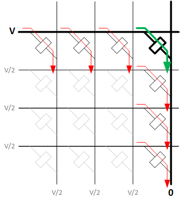
These cells have V/2 across the resistor, either between V and V/2 (selected row) or between V/2 and 0 (selected column). So there will be current through these cells (red arrows) – albeit half the current of the selected cell (assuming a linear resistor). These cells form the sneak paths. The current going through them is irrelevant to accessing the selected cell.
Actually, it’s worse than that. All such sneak current raises the overall energy consumption of the memory. But, in addition, check out the selected column. It will have current from the selected cell, but also from the de-selected rows. In theory, two deselected rows would double the read current – full read current from the selected cell and twice the half-current from the two de-selected rows. (Again, assuming a linear resistor.) With lots of de-selected rows, the current from the selected cell gets swamped.
I don’t want to get too literal about exactly how much current there is, but the point is, the extra current makes the job of reading the selected cell much harder. It would be preferable if there were a way to isolate or select a specific cell in such a way that it provides a current while no other cells provide a current. This additional element is called a selector.
Selecting a Selector
So how to do that? This is a topic that was addressed in a paper by a team from SK-Hynix at last December’s IEDM conference. In theory, you could put a transistor in series with the resistive element, turning the transistor on for only the selected cell. Without that transistor, the row and column voltages provide both current and selection. With that transistor, the transistor does the selecting, while the row and column voltages still provide the sense or write current.
But this is an expensive solution. You have all those transistors, and you need separate decoding to turn them on – in addition to the decoding for selecting rows and columns. Lots of diffusion, lots of wires. Not great. This is what has made the hunt for a selector such a challenge. It needs to be cost-effective.
The team considered so-called ovonic threshold switches. These make use of phase changes to allow or disallow current – just like a CD. But they say that this technology isn’t stable over temperature and that the switching threshold changes with age. (It also seems to me that writing would be slow, but I’m not sure of that.)
Then they looked at so-called programmable metallization cells (PMCs). These are made of a solid electrolyte sandwiched between two electrodes. Those electrodes supply material that can form a filament in the electrolyte, reversibly. Sound familiar? Yeah, it sure feels a lot like the ReRAM cell itself. The aforementioned irony.
In this case of this work, they used a dielectric – SiO2 (heard of it?) – instead of an electrolyte. Which means we’re not talking about a filament; we’ll come back to that in a sec.
For the metal, they tried both copper and silver, and those metals worked well in principle – but for two critical issues. First, their thresholds are too low (we’ll come back to why this is important). Second, these aren’t metals that fab managers are crazy about floating around in their fabs. Too much contamination potential. So, instead, they went with arsenic (As).
What’s critical for this to work – and why Cu and Ag had threshold issues – is that you want this switch to turn on only for a fully selected cell. In other words, it needs to have something greater than V/2 across it for it to conduct. In yet other words, the threshold must be greater than V/2. That way, with the partially selected cells, the switch remains off, suppressing current. Current flows only for the selected cell, solving the sneak-path issue.
This selector is also quite small, solving the cost issue.
Now let’s come back to the filament question. In standard PMCs, the electrodes supply the carriers that form the filament, dissolving into the electrolyte. But, both intuitively and experimentally confirmed, As atoms – and the nanoparticles that they form – aren’t mobile in the dielectric matrix. So they can’t come together to form a filament. That means something else is at work here.
The team worked hard to figure out the As implant dosing and depths so that the atoms or nanoparticles would be evenly distributed throughout the dielectric. They didn’t want large numbers to end up in contact with each other, forming a filament that couldn’t be pulled apart.
So if there’s no filament, then how does it conduct? Their idea, as explained through email by lead author Soo Gil Kim, is that the As interspersed among SiO2 effectively forms a series of bands: SiO2/As/SiO2/As/… between the electrodes. When a field is applied, rather than the As moving around, the bands are distorted, and, above the threshold, they’re able to conduct.
There’s one other step required to get this working. The interfaces between the top and bottom electrodes and the dielectric are themselves insulating. So a forming step is used to break that interface and allow conduction.
What about Speed?
Performance is the characteristic that establishes the intended application for this memory. They found that it takes 23 ns to turn on the switch and 52 ns to turn it off. That means that any memory access can take at minimum 23 ns – 52 ns if a prior cell must be deselected first. Add to that the actual decode time and the cell time and the sensing time, and you’ve got something that’s not going to compete with SRAMs for sure.
And it might get worse. You could hide the selection time behind the deselection time if you could deselect one cell at the same time that another is being selected. The select time of 23 ns would hide behind the simultaneous deselect time of 52 ns, making the overall switchover take 52 ns (plus all other delays). But if you have to deselect before selecting (perhaps there would be something akin to crowbar current in the middle of the transition, and perhaps that would be a problem), then you first have the 52 ns followed by the 23 ns, for 75 ns total transition (plus all other delays).
I asked Mr. Kim about this, and his response is that this memory isn’t competing with, say, MRAM or DRAM or SRAM. It’s targeted at so-called storage-class memory, whose performance requirements are lower.
As to the simultaneous select/deselect question, he said that you can’t have more than one cell selected at a time, since there isn’t enough write-driver current for both cells, and the complexity of the sense amps also makes this difficult. He did say that, while they haven’t tried this yet, some level of overlap might “theoretically” be possible, as shown in the figure below.
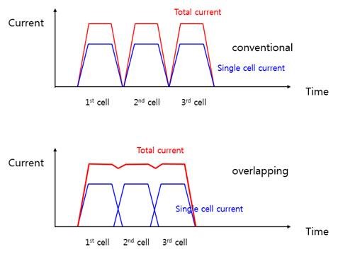
(Image courtesy Mr. Soo Gil Kim, SK Hynix)
In summary, then, these guys may have found a way to sneak a small, fab-friendly selector into a crosspoint ReRAM storage-class memory, keeping access simple and cost-effective.
More info:
“Breakthrough of Selector Technology for cross-point 25-nm ReRAM,” Kim et al, IEDM 2017 proceedings


What do you think of the ReRAM selector proposed by the SK-Hynix team at IEDM?