industry news
Subscribe Now

Leti to Present Latest R&D Results in MEMS At Transducers’ 2013 in Barcelona

GRENOBLE, FRANCE – May 29, 2013 – CEA-Leti will host a workshop for industrial companies to present its latest advances in MEMS and an overview of the success of its recent MEMS startup, Wavelens, during Transducers’ 2013 and Eurosensors XXVII in Barcelona, Spain.

Workshop: 6:30-8 p.m., June 18, Rooms 118-119, CCIB Barcelona

The session features three brief presentations from 6:30-7:10 p.m.:

  • 6:30-6:40 p.m.: Overview of CEA-Leti, from technologies to applications. Jean-René Lèquepeys, head of Leti’s Silicon Components Division, which is involved in micro- and nanoelectronics, micro- and nanosystems, and 3D stacking.
  • 6:40-7 p.m.: Presentation of Leti’s most recent major achievements in the MEMS field, with a focus on advanced multi-purpose MEMS and NEMS platforms. Dr. Julien Arcamone, manager for MEMS business development in the Silicon Components Division.
  • 7-7:10 p.m.: Update on Wavelens, a recent Leti startup that is focused on improving the performance of miniature cameras with innovative MEMS optical solutions. Dr. Arnaud Pouydebasque, Wavelens CTO.

A networking and cocktail event will follow the workshop from 7:10 p.m. to 8 p.m.

Visit www-leti.cea.fr/en/Prochain-evenement/LETI-MEMS-workshop for more details and registration information.

About CEA-Leti

Leti is an institute of CEA, a French research-and-technology organization with activities in energy, IT, healthcare, defence and security. Leti is focused on creating value and innovation through technology transfer to its industrial partners. It specializes in nanotechnologies and their applications, from wireless devices and systems, to biology, healthcare and photonics. NEMS and MEMS are at the core of its activities. CEA-Leti operates 8,000-m² of state-of-the-art clean room space on 200mm and 300mm wafer platforms. It employs 1,700 scientists and engineers including 320 Ph.D. students and 200 assignees from partner companies. CEA-Leti owns more than 2,200 patent families.
Visit www.leti.fr.

Leave a Reply

featured blogs
May 2, 2024
I'm envisioning what one of these pieces would look like on the wall of my office. It would look awesome!...
Apr 30, 2024
Analog IC design engineers need breakthrough technologies & chip design tools to solve modern challenges; learn more from our analog design panel at SNUG 2024.The post Why Analog Design Challenges Need Breakthrough Technologies appeared first on Chip Design....

featured video

Why Wiwynn Energy-Optimized Data Center IT Solutions Use Cadence Optimality Explorer

Sponsored by Cadence Design Systems

In the AI era, as the signal-data rate increases, the signal integrity challenges in server designs also increase. Wiwynn provides hyperscale data centers with innovative cloud IT infrastructure, bringing the best total cost of ownership (TCO), energy, and energy-itemized IT solutions from the cloud to the edge.

Learn more about how Wiwynn is developing a new methodology for PCB designs with Cadence’s Optimality Intelligent System Explorer and Clarity 3D Solver.

featured paper

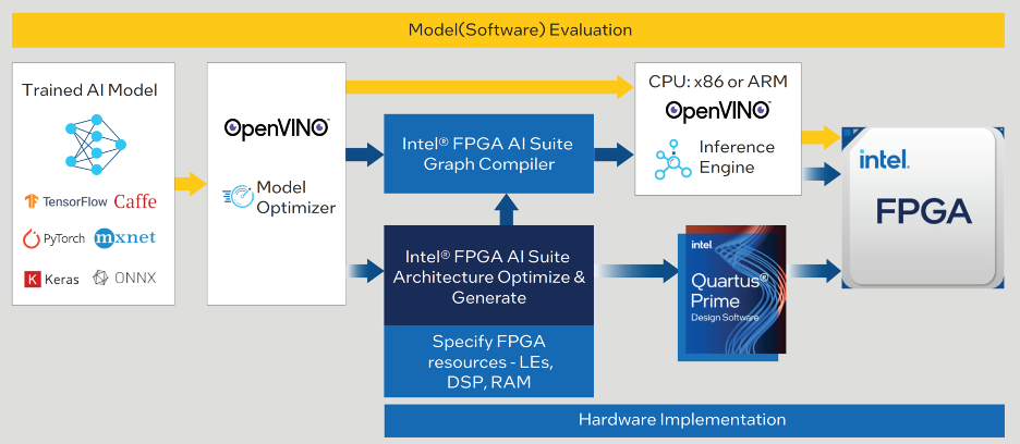
Altera® FPGAs and SoCs with FPGA AI Suite and OpenVINO™ Toolkit Drive Embedded/Edge AI/Machine Learning Applications

Sponsored by Intel

Describes the emerging use cases of FPGA-based AI inference in edge and custom AI applications, and software and hardware solutions for edge FPGA AI.

Click here to read more

featured chalk talk

Achieving High Power Density with IGBT and SiC Power Modules
Sponsored by Mouser Electronics and Infineon
Recent trends in the inverter market have made high power density, scalability, and ease of assembly more important than ever before. In this episode of Chalk Talk, Amelia Dalton and Abraham Markose from Infineon examine how Easy & Econo power modules from Infineon can help solve common inverter design requirements. They explore the benefits and construction of these modules and how you can take advantage of them in your next design.
May 19, 2023
38,464 views